74ls610 replacement board
Table of content
The information within these pages is taken from a 1981 Texas Instruments data book.
I use this chip as MMU chip in my CS/A65 computer, where a schematic can be found how to use the chip in a 6502 computer. An overview how to use this memory mapper can be seen in the System Block Diagram.
There is not much information on this page, as it is more aimed at the general understanding of how this chip works. You are encouraged to get the relevant data from TI - although they are not electronically available (at least a site search didn't reveal anything).
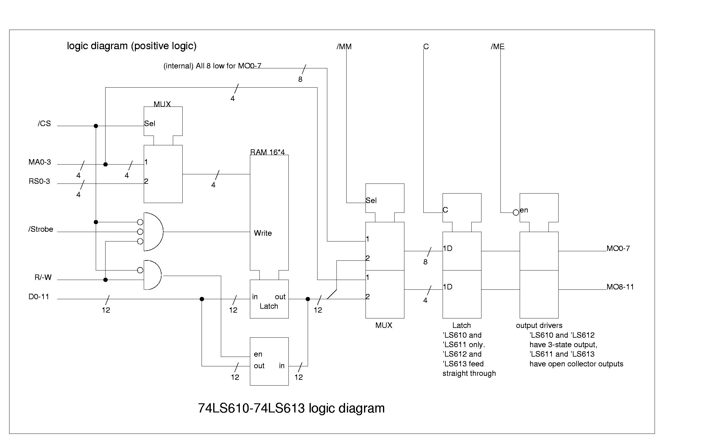
The internal logic diagram can be found in ls610b.png. This shows that the internal RAM is not a dual-port or whatever RAM, but a simple multiplexed register file. This has consequences for the modes of operation.
The address lines for the register file come either from RS0-3 (for
read/write operations) or from MA0-3 (for mapping).
This is switched by the /CS line. Thus, if you access the
read/write port by setting /CS low, you loose the mapped
output. The 'LS610 and 'LS611 have a latch that is controlled
by C and can be used to save the mapped address lines
during a read/write access.
/MM controls a multiplexer that either selects the mapped
address lines as output (map mode), or feeds the input address lines through
to MO8-11 setting the other lines to zero (pass mode).
This input thus enables or disables the mapping.
During read operation the mapped address lines are feed back to the
input D0-11 to allow reading by the CPU. /CS must be
low and R/-W must be high.
During write operation /CS must be low, as well as R/-W.
In addition /Strobe must be low too. This input can be used
for additional timing.
You can read a better explanation in the virtual address space article.
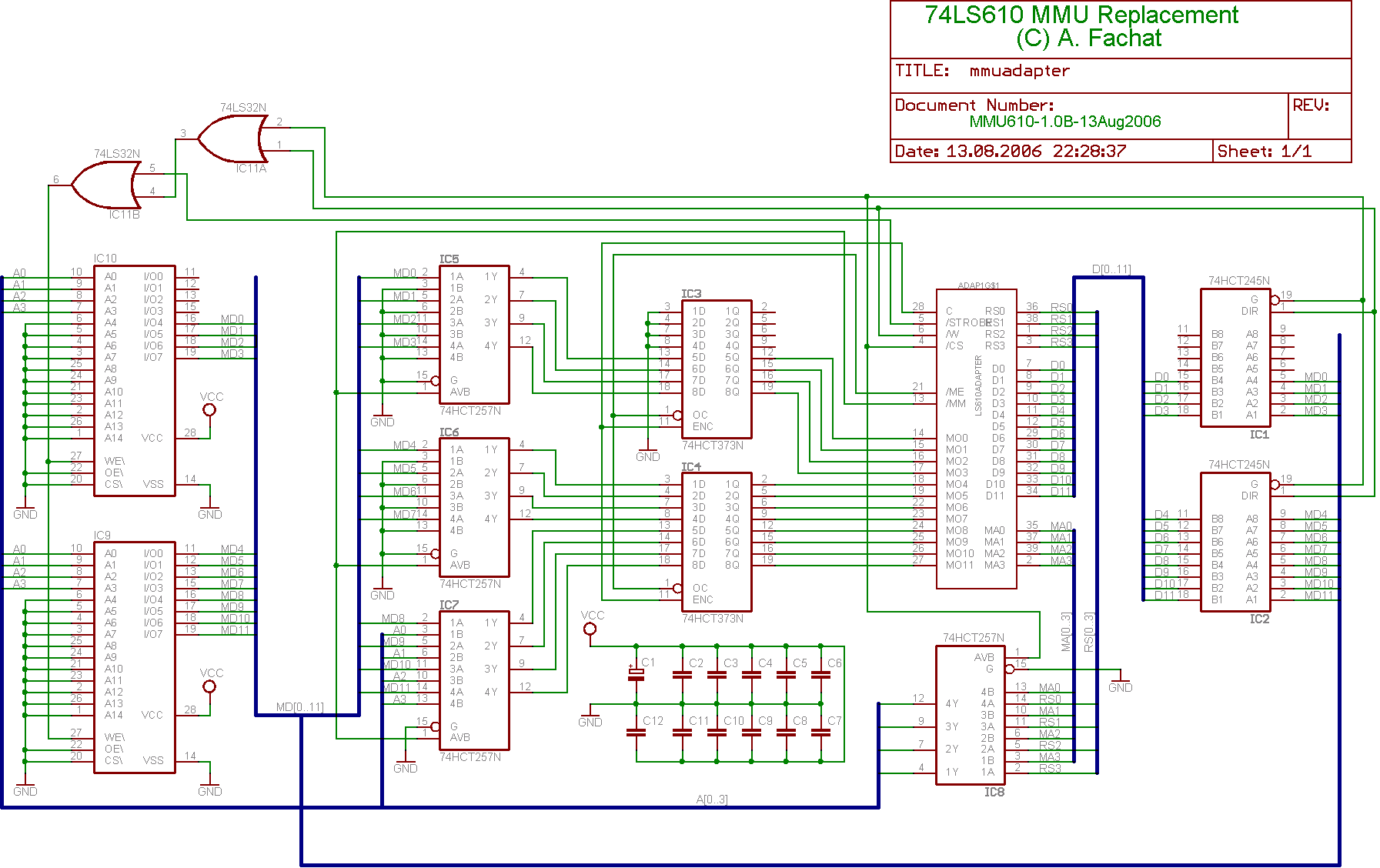
Version: 1.0B
Status: untested
Notes
| This board has the two lines exchanged compared to the 1.0A version. |
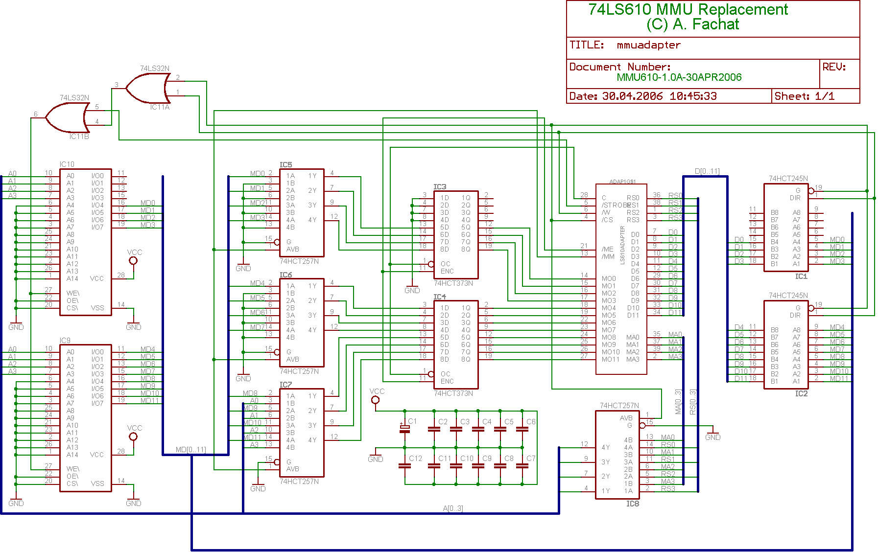
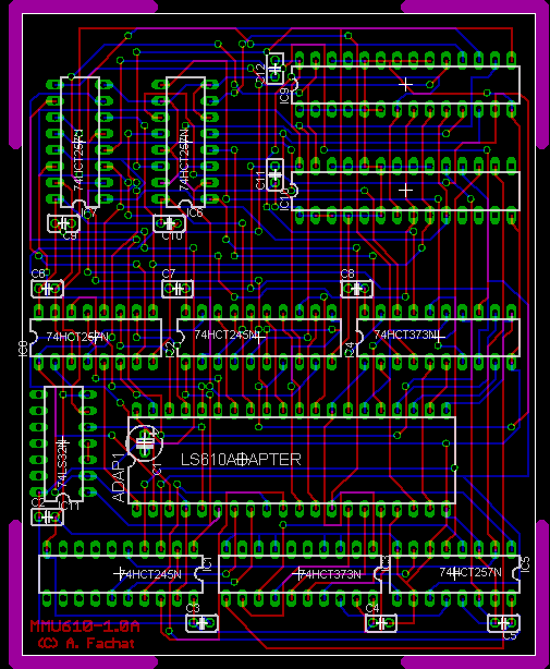
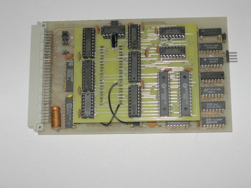
Version: 1.0A
Status: prototype with bug
Notes
In this schematic and board layout has a bug: the two
lines C and /ME of the
74ls610 socket must be exchanged.
|
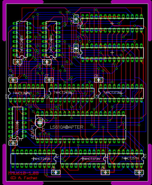
Files
| mmu610_v1.0a.sch | |
| mmu610_v1.0a-sch.png | |
| mmu610_v1.0a.brd | |
| mmu610_v1.0a-lay.png | |
| mmu610_v1.0a.jpg(on top of an old CS/A65 CPU board) |