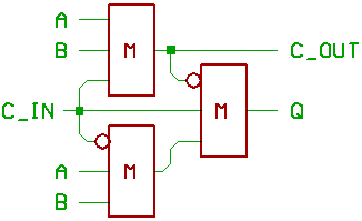
Zhang et al, 2004:
Only three majority gates...
and two inverters.
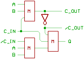
But when feeding through an inverted
and a non_inverted carry, one inverter
per Bit should do:
Now to analyze what happens inside the
circuitry (like we did on the previous page).
If we assume, that the carry input C_IN
is 0, we can replace the majority gates
with simple logic gates:

The NAND gate emits 0, when A=1 and B=1.
The OR gate emits 0, when A=0 and B=0.
So we have the well known XOR functionality
at the Q output.
Now for what happens, if C_IN=1:
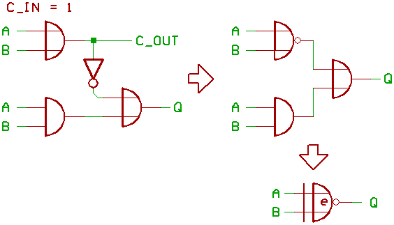
The NOR gate emits 1, if A=0 and B=0.
The AND gate emits 1, if A=1 and B=1.
What gives us an XNOR functionality on Q.
Now for some thoughts on how to build
our small ALU:
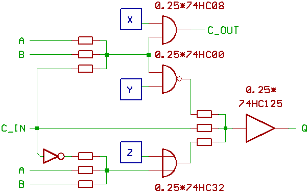
Feeding the inputs of two logic gates with
one resistor network sure won't improve the
propagation delay of the carry chain, maybe
you want to change this...
Arithmetic mode: X=1, Y=1, Z=0.
It will work like the adder described above.
For logic mode, we have to turn of the
carry chain by setting X to 0.
Q = A XOR B: X=0, Y=1, Z=0.
Nothing news here.
Q = A OR B: X=0, Y=0, Z=1.
Y=0 forces one input of the majority gate to 1.
Said gate then passes through A OR B.
Q = A NAND B: X=0, Y=1, Z=1.
Z=1 forces one input of the majority gate to 1.
So the majority gate passes through the output
from the NAND gate to Q.
Problem is, that there isn't an AND function,
looks like you would have to perform A AND B
in two steps: first A NAND B, second to invert
the result, maybe by performing a logic XOR
with "-1" (0xff for an 8 Bit ALU).
[HOME] [UP]/ [BACK] [1] [2] [3] [4] [5] [6] [7] [8] [NEXT]
(c) Dieter Mueller 2009