A proof, that building an ALU with multiplexers really works.
I'm now drawing things a bit different from the 74381/74382
datasheet, simplifying the one or other part.
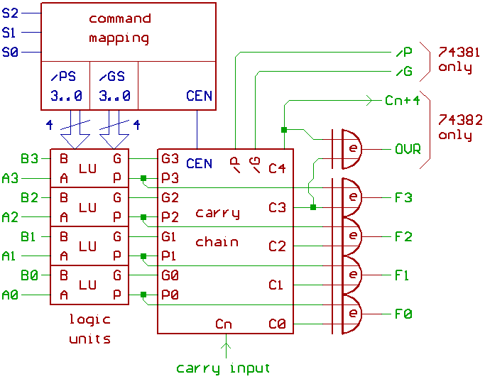
Basically we have a 4 Bit ALU, that consists of four one Bit
logic units (which emit the propagate signals P and the generate
signals G), some circuitry labeled "command mapping" to convert
the three control signals S2..S0 into the 8 control signals which
configurate/drive the logic units... plus the CEN signal,
which enables the carry chain in arithmetic mode.
Oh, and I nearly forgot to mention the XOR gates which are fed
by the propagate signals and the carry chain.
74381 emits /P and /G signals, what makes this IC interesting
for building fast/big ALUs by linking said ICs together with a 74182...
which is described later in this article.
74382 lacks the /P and /G outputs, but features a carry and overflow
output instead, what will do for building 8 Bit ALUs.
Now to take a look into the boxes which are labeled "logic unit".
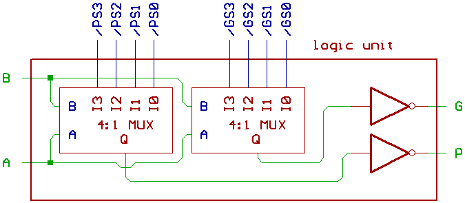
/PS3..0, /GS3..0 have to be low_active, because the multiplexers
have inverted outputs.
A list, of what operation the ALU should do according to the
S2..S0 control signals... and what the control signals inside
the ALU should look like to make this possible:
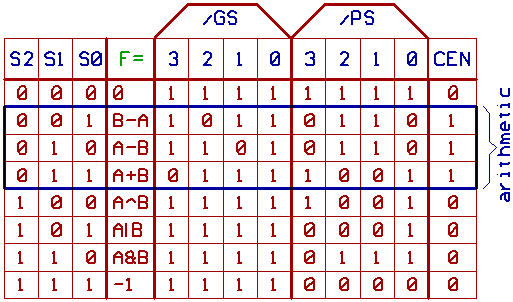
And here the circuitry that turns S2..0 into said signals:

Note, that /GS1 always is 1.
[HOME] [UP]/ [BACK] [1] [2] [3] [4] [5] [6] [7] [8] [NEXT]
(c) Dieter Mueller 2012