 ---------------------------------------------------------
| To boldly go, where no other hobbyist had been before.  |
| On second thought, maybe nobody made it back from there |
| with enough mental health left to tell the story,       |
| that probably would explain quite a few things.         |
 ---------------------------------------------------------
MT15 featured flipflops, built with NAND gates using saturating logic.
While trying to build smaller/faster transistorised flipflops,
I figured out that DECL flipflops would take 40 percent less PCB space,
while being a lot faster, at nearly the same power dissipation.
For instance, a saturating master/slave flipflop with BC547/BC847 in MT15
was limited to ca. 4 MHz, while a non_saturating DECL master/slave
flipflop with the same transistors could still work at 20 MHz.
And now, I wanted to know.
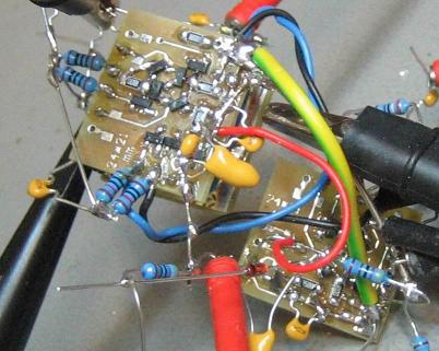
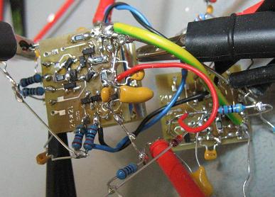
Pictures from a 15 MHz test run with BFR93A transistors.
Had to terminate the flipflop outputs with 100 Ohm resistors to -1.8V,
to prevent the flipflops from turning into oscillators.
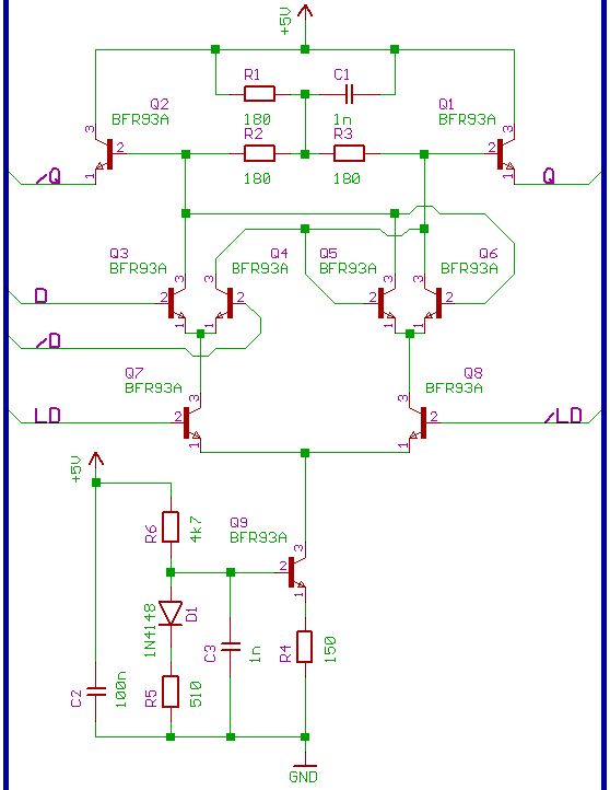
Right side: single ended ECL (SECL) to differential ECL level (DECL) converter.
Left side: two transparent DECL latches, wired up as a master/slave flipflop.
Imagine a half 74F74, with !Q connected to D, working as a 1 Bit binary counter
dividing the clock frequency by two.
Some more pictures:
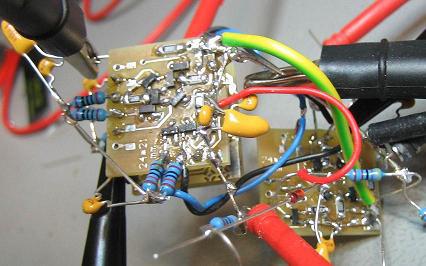
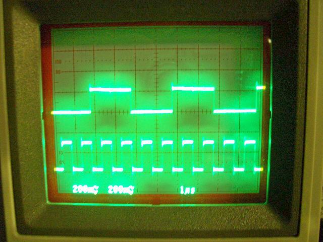
Decided to buy a 100MHz TTL crystal oscillator, and to connect it to the
SECL to DECL level converter by using a capacitive voltage divider.
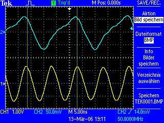
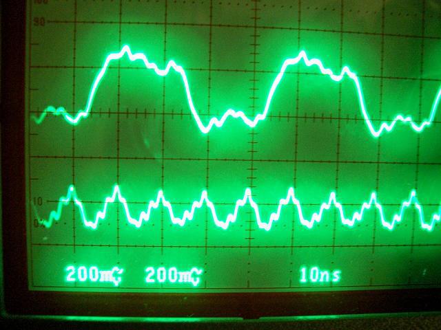
Please don't take too much attention to signal shape/amplitude and such.
I only had a cheap 200 MHz oscilloscope and lousy 100 MHz passive probes.
But fact is, that it did divide 100 MHz by two, and that the speed is more limited
by wiring, PCB layout and test equipment, than by the transistors themselves.
...Another planet conquered by Spaceman Spiff.
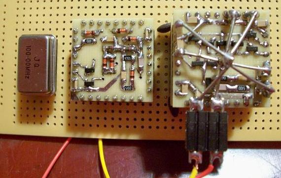
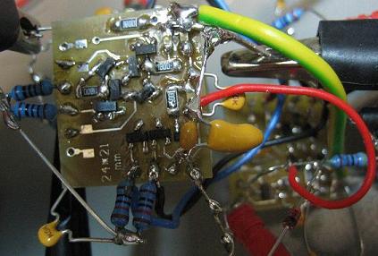
Left: 100 MHz TTL oscillator.
Middle: TTL to DECL level converter.
Right: four transparent DECL latches.
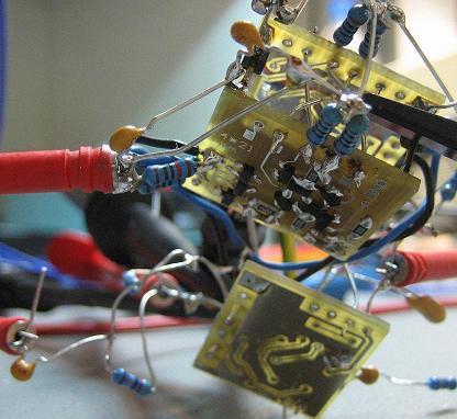
Now for the module on the right:
Yep, 4 identical PCBs, rotated in 90 degree steps
and soldered together to a "tower".
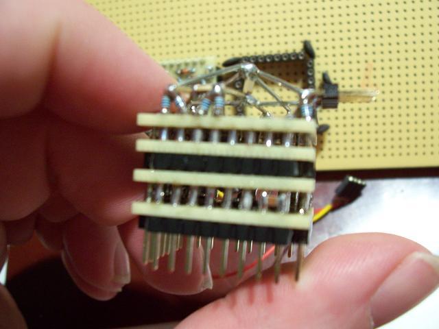
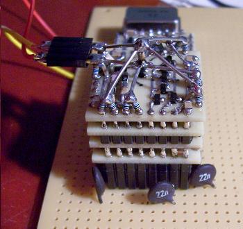
The breadboard PCB connects the 4 latches together
to make them work as two master/slave flipflops,
dividing a frequency by 4.
Looks like half an inch of "open" wire makes a difference,
had to place termination resistors on top of the module,
and there also are termination resistors at the bottom
of the "backplane" PCB.
BTW: Tektronix 2467B.
I'm not happy with the PCB layout of the flipflops,
looks like something tries to oscillate in there.
The concept/schematic is a bit different from what I
had back in 2006, and the flipflops are now powered
with +5.0V instead of -5.2V.
Unfortunately, changing the supply voltage happened
a bit late during the design process, and because of this
the TTL/ECL and ECL/TTL level converters are prototypes
which don't work reliable.
Conclusion:
It might be possible to homebrew sub_nanosecond logic
when investing some more time/effort into PCB layout,
but distributing the signals would be going
to be tough.
Especially if you would try to build something big,
like a CPU. And long (impedance controlled) wires/traces
are killing speed.
For instance, when using CAT5 Ethernet cable, the signal
might travel at 65% of "the speed of light" through the
wires... in other words, ca. 19.5 centimeters per nanosecond,
or 2.5 ns for half a meter of wire.
It turned out, that it's possible to reduce the propagation
delay of a MT15 NAND gate to ca. 5ns when reducing the resistor
and capacitor values by 50% and replacing the BC847 by a BSV52
(both transistors have identical package and pinout).
So I started to think, that DECL probably won't be worth the
trouble, and all DECL research came to a grinding halt.
ECL/DECL lessons learned so far:

1)  Keep control/data input lines from the "outerworld"
    to transistors on the PCB as short as possible.

2)  Try to keep things symmetrical, which means that
    PCB traces for LD,/LD etc. of a flipflop should
    have equal length. If you go beyound 30 MHz and
    you don't take care of that, you're asking for
    trouble.

3)  Be aware, that vias in your PCB act as inductors
    at high frequencies, so try to avoid them in your
    signal lines.

4)  "Emitter coupled logic" is just a figure of speech.
    Thou shalt not directly tie together the emitters
    of the transistors in your differential amplifier,
    and then "attach" the the resistor (or transisor)
    for setting the current somehow.
    Better route traces (at equal length) from the
    emitters to said resistor/transistor !

5)  Watch your GND distribution/connection !
    Reliability of your design will stand or fall with
    that !

6)  PCB layout will be a compromise, you probably may
    notice that points 1) to 5) will rarely overlap.

7)  Watch the GND connections from the signal generator
    and the oscilloscope to your circuitry, at high
    frequencies it _does_ matter how (and _where_)
    GND from said devices is wired to your circuitry.
    Andrew Holme has a nice application note on his
    homepage about high speed comparators, which gives
    you a few hints.

8)  If your flipflop refuses to work, there is either
    something wrong with the DC levels of the input
    signals, or with the length of your wires/traces.
    Note, that at high frequencies, half an inch can
    make the difference between sucess and failure...
    also watch out for line reflections.

9)  Common mode rejection and parameters of a differential
    amplifier change with the DC level of the input signal,
    if you are not using constant current.
    Especially when building line receivers.

10) Try to go for a 2.6 mA current for your differential
    amplifier. Be aware that there seems to be a 1:12 ratio
    for the collector currents of the transistors in the
    amplifier, which means that 2.4 mA will flow through
    the "active" transistor, and 0.2 mA through the "inactive"
    transistor... which might cut off at a lower current,
    what will confuse your ECL/DECL logic gate pretty much.
    You could go for more current of course, but better
    check if this affects the input signals of said
    amplifier.

11) If you happen to have two ECL/DECL gates on a PCB,
    and you use one resistor based voltage divider for
    setting the reference voltage for the "constant
    current sink" of_both_ gates (to save PCB space
    and components), be aware that if the voltage
    levels at the input signals of one gate won't be
    correct (open inputs etc.), it would affect the
    reference voltage for both gates, so they both
    will act strange.

12) BFR93A/BFT93 transistors are used in input amplifiers
    of oscilloscopes, so you probably need something faster
    (or better) than a 400 MHz oscilloscope to figure out
    what actually happens in your circuitry.

13) Try using BC847/BC857 low frequency transistors for
    your first experiments, at a 20 ns propagation delay
    there is a winning chance when using a 100 MHz
    oscilloscope. BFR93A/BFT93 has identical package
    and pinout to BC847/BC857, so you don't have to
    change your PCB layout when using fast RF transistors
    later.

14) BFR93A/BFT93 certainly are less robust than BC847/BC857.
    If one of the transistors inside a logic gate dies,
    you better replace all of them.

15) Propperly distributing a fast DECL signal through
    impedance controlled traces is tough. Try to dig
    through LVDS application notes to get some hints
    on how to distribute/terminate DECL signals.
    Notice, that you might have to invest some years
    of getting the practice/experience for being able
    to build a "proper/reliable" solution.

16) Note: the fastest frequency on a signal line might
    be determined by the rise/fall time of the signal.

17) If you really should try building your own DECL based
    computer, better check the price for 6 layer PCBs first.

18) Be aware, that electrons might travel through impedance
    controlled traces slower than through vacuum.
    (Some old oscilloscopes like the Grundig MO50 used PCB
    traces as a delay line.)

19) If in doubt, try to investigate how Seymour Cray would
    have solved the problem.

20) Building transistorised ECL/DECL is a lost art, so
    don't expect much help from others when you're in
    trouble... and be aware that "trouble versus help"
    might be inversely proportional, too.

21) Digging through service manuals of old oscilloscopes
    (Grundig) and function generators (HP) could give you
    some ideas, also try searching for patents.
    Old Motorola ECL datasheets might be interesting to
    read sometimes.

22) From what I have seen, visiting a university for five
    years will not prepare you for the things to come,
    it's just a starting point.
    It's like you had a beginner course in playing chess
    (what figures are on the playfield and how to move them),
    and you suddenly stumble into a game with Kasparow.
    Take care.

23) There isn't a clear border between analog and digital
    design.
    Especially when using transistors.
    Especially when aiming for speed.

24) Try to have a clear concept of what you're doing before
    running simulations. If you run simulations first,
    then make a design and try to resort to common sense
    later, you probably won't go far.
    The mightiest design tools are paper and pencil...
    not the fastest design tools, of course.

25) Transistorised ECL/DECL logic is a nice playground
    for wasting time, money and components in a creative
    way.

26) If someone who might have more experience than you
    tells you what things to avoid, consider that it might
    have taken him some time and money to figure that out
    in the past. If you don't listen, you're going to
    waste some time and money in the future...
(c) Dieter Mueller 2006..2008