'X' stands for "experimental", what is different from "production quality".
Estimated speed might be ca. 2 MHz with 74HCT,
but the ICs used in here are supposed to be avaliable as 74ACT... somewhere.
  ---------------------------------------------------------------
 |No plain fanfold paper could hold that fractal Puff.           |
 |He grew so fast no plotting pack could shrink him far enough...|
  ---------------------------------------------------------------
Trying to do logic design at a certain degree of complexity
while getting raked by crackers\spammers
pretty much feels like
trying to repair a mechanical wrist watch
while getting raked by artillery.
So just running the project to the point where I could do
a "core dump" of what I have so far took 5 years
(when counting those unvoluntarily taken "breaks").
Initially, X02 was supposed to become a transistorized CPU.
After a while, plans were cut back to building a mere TTL CPU.
Eventually, I had no choice but to cancel the whole project.
Basically, X02 now is just another "paper design".
So be warned, that the schematics on this page are untested,
probably full of errors, and in no way optimized for speed or compactness.
It may take you more than two years of hard work to turn all this stuff
into something "useful"... whatever that means.
It's just a "core dump" of a work which had been in progress
while getting cancelled.
I'm not sure, if converting this design to VHDL
would be worth the effort\trouble.
So X02 only would be interesting for you if you are out
to build a TTL or transistor implementation of a 6502
without resorting to microcode.
X02 supports the 65C02 instruction set,
plus 23 instructions from the 65816:
TXY
TYX

BRL

JSR (ABS,X)

PEA
PEI
PER

ORA d,s
AND d,s
EOR d,s
ADC d,s
LDA d,s
STA d,s
CMP d,s
SBC d,s

ORA (d,s),y
AND (d,s),y
EOR (d,s),y
ADC (d,s),y
LDA (d,s),y
STA (d,s),y
CMP (d,s),y
SBC (d,s),y
d,s feels similar to z,x
except that "data is relative to SP and in page 1".
(d,s),y feels similar to (ind),y
except that "pointer is relative to SP and in page 1".
The plan was, to fork the design into X03 later.
X03 would have had a 24 Bit address bus and a 16 Bit direct register
(following the M02 instruction set architecture).
// a "poor man's 65816 without the 16 Bit
Since there is a big "gap" between 65C02 and 65816 architecture,
I would have needed something like X03 as a "stepstone"
when trying to aim for the 65816 someday.
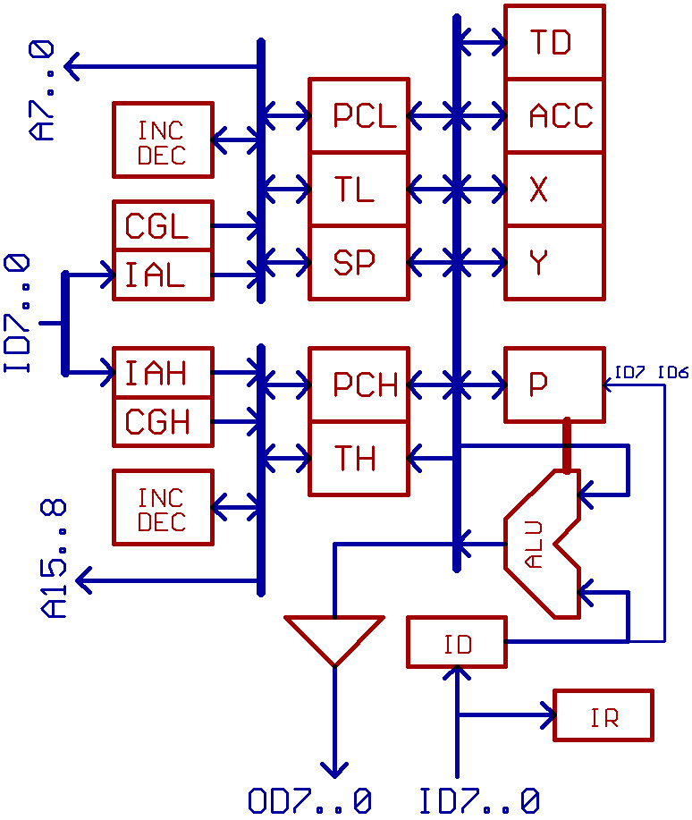
Now for a block diagram of the mill:
Internal address\data_bus, ALU, registers.
A15..8, A7..0 connect to the external address bus.
ID7..0 and OD7..0 connect to the external data bus.
Simplified concept:
Actually, busses in X02 are uni_directional:
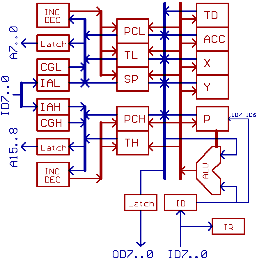
Boxes which are labeled "Latch" are transparent latches,
their main purpose is to improve bus timing.
For understanding the basic X02 concept just ignore them for now.
IAH, IAL are registers between external data bus and internal address bus.
CGH, CGL are constant generators, to be used
when fetching interrupt vectors or when accessing page 0 or page 1 in memory.
TH, TL are temporary registers, mainly used for address calculation.
TD is a temporary date register to be used for read/modify/write operations.
P is the status register.
ID is the data input latch.
IR is the instruction register.
Unlike most other 6502 "compatible" TTL implementations,
X02 doesn't use a counter for incrementing PC.
Instead, it has a 16 Bit incrementer\decrementer
for incrementing/decrementing PC and SP.
Now for an example:
While executing a JMP instruction, PCH:PCL feeds the internal address bus,
and PC is incremented while the two Bytes containing the jump address
are fetched into IAL, then IAH from external data bus.
When fetching the next instruction from the external bus,
X02 feeds the internal address bus with IAH:IAL (instead of PCH:PCL),
this address is incremented and written into PCH:PCL.
X02 makes extensive use of such little tricks during address calculation.
Now for the instruction decoder\sequencer.
...Microcode ? What microcode ?
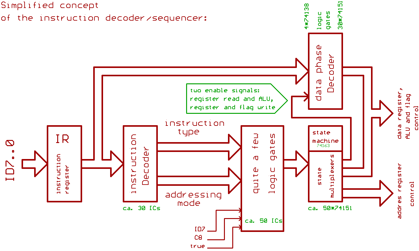
The instruction decoder (ca. 30 TTL ICs)
dissects the Byte from the instruction register,
identifying instruction type and addressing mode.
Next, we have a little lump of logic gates (ca. 50 TTL ICs),
generating some "product terms" out of instruction type,
addressing mode, ALU carry output etc...
(When using a FPGA, you could implement most of those two function blocks by using a lookup table).
Next, we have a 4 Bit state machine,
basically a 74163 counter, counting from 0 to 8.
The control signals which enter the pipeline
(control signals drive the mill in the next machine cycle)
are generated by a lot of 74151 8:1 multiplexers
(one multiplexer per control signal).
Multiplexers are fed by the state machine counter,
and by those "product terms" who are generated by that
odd lump of logic gates.
BTW:
For some of the control signals, it requires less circuitry
to focus on product terms where the signal is inactive
(like when loading the data input latch).
You would need to tap into the inverted output
of the multiplexer then, of course.
The basic idea was, that executing 6502 instruction set
is broken down into two parts:
0) "data phase":
Either a machine cycle, in which the ALU reads a register,
performs an operation, writes a register and modifies the flags,
including BCD correction in decimal mode.
Or a machine cycle, in which a register is written into memory,
like the write cycle in STA, STX, STY etc.
This also includes the write cycle in read/write/modify operations
like when incrementing/decrementing/shifting a Byte in memory.
1) The rest
Including address calculation sequence, reset\interrupt sequence,
sequences for jumps, calls, returns etc.
;...................................................................
For instance:
LDA ABS would read a Byte from memory, pass it through the ALU, then write
it into ACC while modifying the flags.
LDX ABS would read a Byte from memory, pass it through the ALU, then write
it into X while modifying the flags.
Both instructions use the same addressing mode
(the same state machine sequence that is),
both instructions pass the Byte through the ALU and modify the flags in the same way.
The only remarkable difference is that the ALU output is written
into a different register.
Now for something funny:
1) A CPU register might be read while ALU "data calculation".
2) A CPU register might be read for STA, STX, STY etc.
3) TD (temporary data register) might be read for writing the result of a
read/modify/write instruction back to memory.
While examinig the OpCode Bit patterns, it suddenly became obvious
that for all those three cases above the circuitries for reading
a CPU register into ALU (or for writing it to memory)
only do conflict for TSB, TRB.
So I decided to use just one circuitry for all three cases
for selecting what register to read during "data phase".
Note, that when writing a register to memory,
the ALU output (and thus the ALU control signals) is irrelevant.
While further minimizing circuitry, it appeared that
PHA, PLA etc. also have a "data phase".
Technically, this also is true for PHP and PLP.
Instructions like CLC, SEC etc. also have a "data phase",
in which the ALU emits either 0x00 or 0xff,
to be written into one of the flags in the status register.
To make a long story short:
The box labeled data phase decoder (ca. TTL 60 ICs)
is nothing but a lookup table with output enable.
The idea was, that a control signal from a multiplexer in the state machine sequencer
just tells the data phase decoder to take over ALU, flag and register control,
and to make them "do things" according to the Byte from the instruction register
during "data phase".
What complicates things a bit is, that BCD correction in decimal mode
requires an additional cycle after the ALU performed the calculation,
and during BCD correction, the ALU inputs (including the carry input)
should not change for getting a correct result.
So I ended up with two different output enable signals
for the "data phase decoder":
One signal, which enables data phase decoder ALU and register read control,
and another signal which enables register write and flag write control.
Now for the flow diagrams, what is supposed to happen when.
It's amazing to watch, how a little bit of pre_emptive register loading
and pre_emptive address calculating shrinks down address calculation
for all those nifty addressing modes related to LDA, LDX, LDY, STA, STX, STY etc.
to just six innocent looking little boxes in the state machine diagram.

Instructions with addressing mode 'implied' take two machine cycles.
Instructions with addressing mode 'immediate' take two machine cycles.
So the state machine handles both addressing modes in exactly the same way.
Some circuitry in the instruction decoder identifies One_Byte_Instructions,
and just prevents that PC is written with PC+1 in cycle '1'.
That's the only part of the control circuitry that is not pipelined.
BTW:
In the NMOS 6502, there seems to be some circuitry tied to the instruction register
which seems to identify One_Byte_Instructions.
Quite interesting, isn't it ?
TD (temporary data register) is set to 0 in cycle '1',
because the STZ instruction stores the TD register to memory later.
(Did steal this idea from Mike Barry's 65m32 concept.)
Now for part 2:
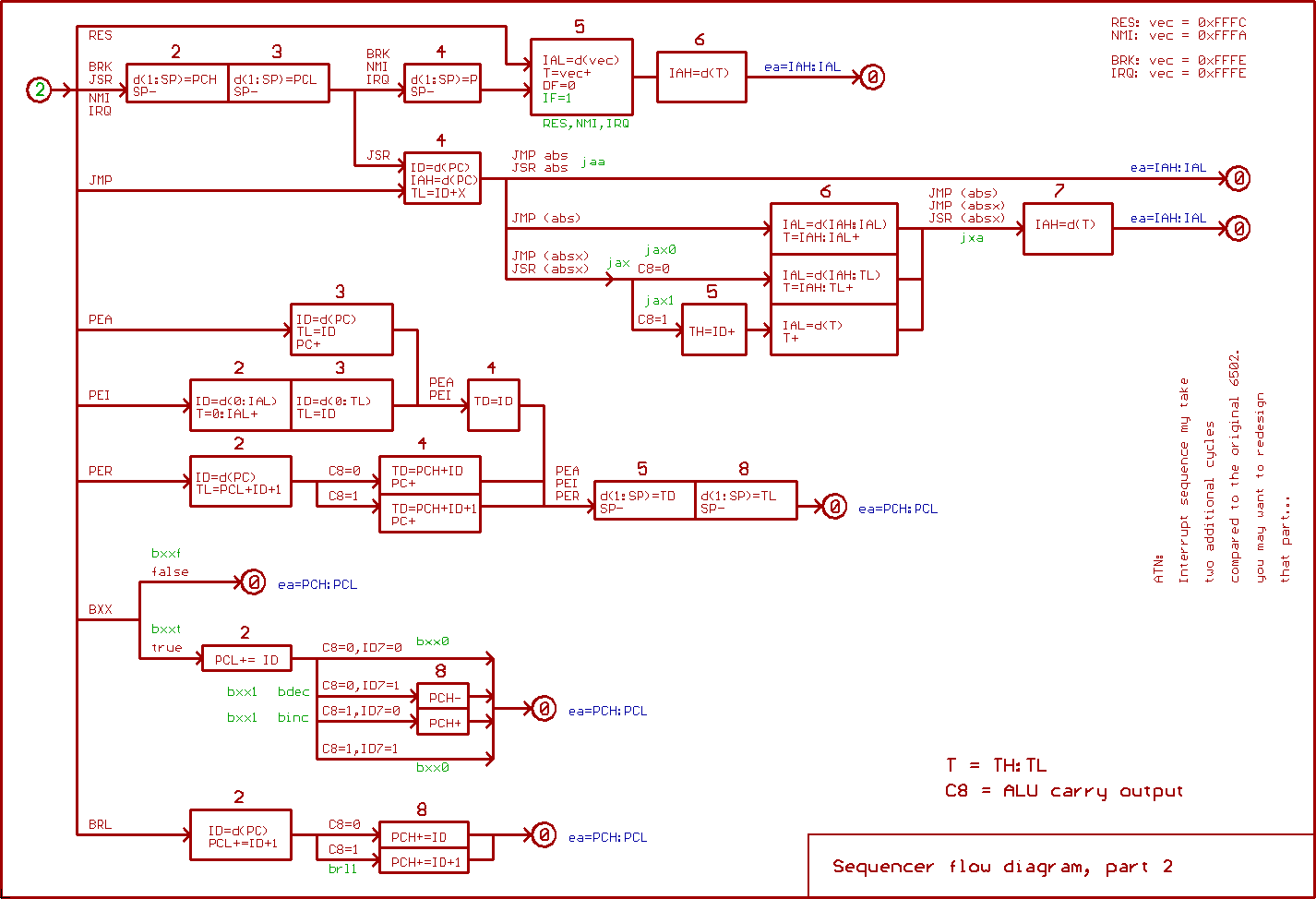
According to the signal named "true", a conditional branch is either
taken or not taken. The signal is generated by a 74151 multiplexer
(controlled by Bit 7..5 of the instruction), which reads the flags
from the status register.
If Bit 4 of the instruction is 0, the "true" signal is forced active.
This covers the un_conditional BRA instruction.
Ok, using/abusing TL as a temporary data register for PEA, PEI, PER
isn't a clean solution...
Added PEA, PEI, PER pretty late to the design after realizing
that implementing stack relative addressing modes won't be much fuss.
Illegal OpCodes will be absolutely different from the 6502, of course.
Maybe you should do a redesign to make X02 handle illegal OpCodes like a BRK.
This might give people a chance of emulating the missing opcodes by software.
BTW:
It's a pipelined design, you need "to think one cycle ahead"
when using those diagrams to generate product terms.
The connections between the boxes and placement of a box into a
certain "slot" in the diagram might be more important than
just reading the text inside those boxes.
Don't get distracted, take care.
Out of a gut feeling, I would dare to say that further optimisation
of those diagrams above might be possible... but thinking _hurts_.
Technically, having a second accumulator and the XBA instruction
isn't a big thing, I just skipped that part when planning X02.
What you would be going to need for handling XBA is:
1) another data register (accumulator) named B (1*74574).
2) instruction decoder\sequencer should generate a signal when detecting XBA.
3) signal should toggle a flipflop, maybe when fetching the next instruction.
4) a 74157 multiplexer is controlled by said flipflop.
5) said multiplexer swaps read/write control signals for registers A,B.
Basically, it's similar to the mechanism used in the TREX CPU for "swapping" register 6 with register 7.
Diagrams for the "data phase decoder" lookup tables can be found
in the project files,
but you would need Eagle PCB layout software to open x02b.sch.
But be warned that my lookup tables probably contain some errors.
I'm suggesting to take OpenOffice or Excel,
then to make a detailed list of instructions which have a "data phase",
how they read/write registers and flags, how they control the ALU etc.,
then to export the list as a plain CSV text file.
The next step would be to "haxor" a little C program which generates
VHDL source code for lookup tables out of that text file...
It also might be interesting to "haxor" sort of a "graphical front end"
for state machine diagrams which also exports into that CSV text file...
It doesn't have to be an "Inkscape plugin", some crude tool running in a
DOS text box probably would do.
Something you should redesign is interrupt handling.
In the implementation on this page, X02 interrupt response
takes two more clock cycles compared to the original 6502.
To simplify the design, I _always_ increment PC in cycle '0',
and to compensate for this, I'm decrementing PC in cycle '1'
if an interrupt was detected.
For a TTL implementation, using a 74163 counter as a sequencer
looks like the best choice.
But for a FPGA or transistor implementation, it could be interesting
to try if replacing the counter with sort of a shift register would result
in a further simplification of the "product terms".
Wikipedia: Schrittkette.
No English version of this text available on Wikipedia, sorry.
"Schrittkette" is a German word, used when implementing
a sequencer by using flipflops forming sort of a shift register
when writing PLC code.
Point is, that during 16 Bit address calculation we have to "insert"
an additional machine cycle when there was a carry when calculating
the lower 8 Bits... for incrementing/decrementing the upper 8 Bits
in the next clock cycle.
Another idea for speeding up a FPGA implementation would be
to do flag modification one cycle after an ALU "data phase operation"
by just holding some of the ALU input and output signals in latches.
This would break the "lenght" of the signal path for generating the V_Flag.
Unfortunately, this also probably would break with the concept
of executing "branch not taken" within two clock cycles...
BTW:
What "the world could need" would be a BSR instruction,
a mix of BRL and JSR for calling subroutines.
In the TTL implementation of X02 on this page,
there are transparent latches between internal and external address bus,
mainly to improve bus timing.
But I forgot to mention that they freeze during address or data calculation
to prevent having garbage on the external address bus by accident.
Problem is, that a "stray read" during "data phase", during read/modify/write
or during address calculation might affect flags in 65xx peripheral chips,
take care.
In a FPGA implementation, there would be two options:
Either to freeze the flipflops in the control pipeline
which are responsible for address register output enable.
Or to store the effective address back into TH:TL
by passing it through the incrementer... by not incrementing.
Also, I started to wonder why I didn't write the result of BXX and BRL
into PCH:PCL instead of writing it into TH:TL.
Compared to the 65816, PEA and PEI take an additional cycle.
This can be fixed if the data input latch ID can be read from
the internal data bus.
Maybe this also would simplify the ALU related equations a little bit,
because then we only would have to increment/decrement/shift
only one of the ALU inputs instead of both of them.
It's an interesting question, if a VHDL implementation
of the X02 instruction decoder\sequencer could be compacted
into one big lookup table feeding one level of "logic units",
(or macrocells) because the address inputs of the lookup table
would change only after instruction fetch...
Maybe somebody someday could build sort of a barrel processor...
but this wouldn't be my battle anymore, sorry.
It's a pity, that for some of the kids nowaday
making easy money at other people's cost
is more interesting than toying with technology.
If something you systematically do
leads to supression of technical knowledge
and puts an end to cool hobby projects,
what are you good for as a "hacker", anyway ?
Good luck and god speed,
I'm out.
(c) Dieter Mueller 2015
BTW: the secret involves not watching TV and staying away from "social media".