Now to describe the logic gates, used in MT15.
Did first experiments with BC547/BC557 transistors at a 5V supply.
The story, how it came to BC847/BC857 SMD transistors powered
with 2.5V would fill a complete article.
Point is, that PCB size is a primary cost factor.
Did not notice any difference between standard BC547/BC557 and
SMD BC847/BC857 in electrical parameters during experimentation.
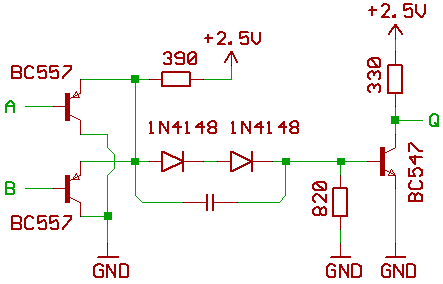
Most of the logic gates used in MT15 are open_collector TTL NANDs.
(TTL = transistor transistor logic).
Note the speed_up capacitor in parallel to the two 1N4148.
220pF should work, but since it was difficult to buy them in a
sort of 0204 SMD package, I did solder 1nF capacitors instead.
NAND means "negated AND". So if A=HIGH and B=HIGH, Q=LOW.
Treshold voltage at the inputs is about 1.3V, so connecting them
to outputs from 74xx integrated logic ICs shouldn't be a problem.
When connecting the output of the transistorised logic gate
to 74xx logic, please use 74HCT/74ACT.
74LS/74F would require a modification of the pullup_resistor
at the output.
Under optimal test conditions (2.5V supply, A,B are driven with
74xx, low capacitance at Q, etc.), propagation delay from A,B to Q
is around 35ns.
Under "real_world" conditions, with long PCB traces, expect
something between 50..60ns.
Supply voltage should be 2.4V to 2.6V.
Don't forget to place one 100nF capacitor into the power supply
of each logic gate.
Now for another neat trick:
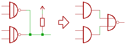
Since the gates have open_collector outputs, it is possible
to wire the outputs from multiple gates together to one single
330 Ohm pullup resistor.
The result would be a AND/NOR combination.
MT15 makes use of this feature.
For more examples what to do with AND/NOR,
please consult/dissect old 74LS/74S datasheets.
Now for something pretty evil:
CTL, complementary transistor logic.
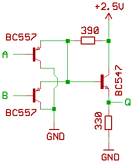
Basically, we take the PNP intputs from our NAND gate,
and attach a NPN transistor.
The rest is known from ECL emitter dotting.
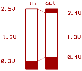
Trick is, to select the pullup/pulldown_resistors in a way,
that a 1.3V input signal level may result in a (nearly) 1.3V
output signal,
for keeping/maintaining treshold level of the
TTL logic gates connected to the output.
Now for some neat open_emitter wiring:
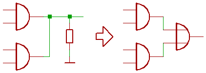
MT15 uses such things inside the carry logic,
and in the instruction decoder/sequencer.
CTL is fast, but has three disadvantages:
There is a chance to waste/burn more energy than with ECL,
it collects (and passes through) any "dirt" at the input signals.
And, since there are no inverters, it doesn't amplify.
Please don't take the picture above too optimistic,
it's for 3.3V CTL..
2.5V CTL has a maximum output level of ca. 1.85V.
Connecting more than three such AND/OR combinations
in series could be considered to be a bad strategy
for building a reliable design.
[HOME] [UP]/ [BACK] [1] [2] [3] [4] [5] [6] [7] [8] [NEXT]
(c) Dieter Mueller 2005