To start simple:
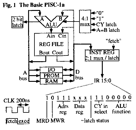
Back in 1994, Bradford J. Rodriguez introduced the PISC1:
This diagram is reproduced subject to the following copyright notice:
From the Proceedings of the 1994 ACM Symposium on Applied Computing.
Copyright (c) 1994, Association for Computing Machinery. Permission to copy
without fee all or part of this material is granted provided that the copies are
not made or distributed for direct commercial advantage, the ACM copyright
notice and the title of the publication and its date appear, and notice is given
that copying is by permission of the Association for Computing Machinery.
To copy otherwise, or to republish, requires a fee and/or specific ermission.
The design shows a stunning simplicity:
There is sort of a bi_port register file, the outputs feed the (74181 based) ALU
and connect to address/data bus.
So it's possible to place the contents of a register (which we may call the
address register) to the address bus, while transferring data between memory and
another register (which we may call the data register), while the ALU is capable
to increment/decrement the address and to write the result back into the address
register.
Note, that all registers can be used as address or data register.
If memory is inactive, the ALU can perform an operation between two registers,
and write the result back into the register file.
Actually, the 74172 isn't exactly a bi_port register file, but nothing in the
74xx family comes that close.
Problem is, that the 74172 is supposed to be extinct, and getting hands on
such ICs could turn out to be impossible for the mere mortal.
Since one 74172 contains eight 2 Bit registers, you would need eight such ICs
for building a 16 Bit CPU.
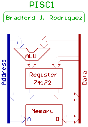
Back in 2003, Andrew holme did decide to use the PISC architecture for building
his second TTL CPU.
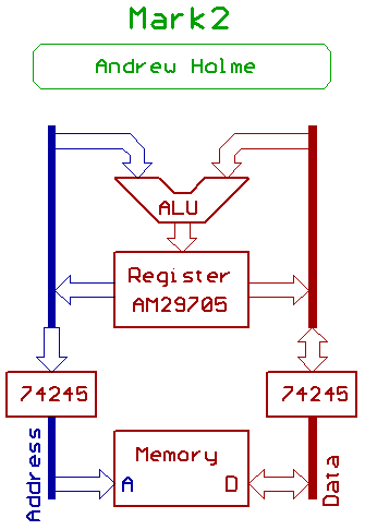
It uses four AM29705 as register file.
The AM29705 was part of the (now extinct) AM29000 family of Bitslice ICs from
AMD, and it was designed to add sixteen 4 Bit registers to an AM29203 or such.
Note, that the AM29705 has only one data input, and two data outputs.
Address and data bus outside the CPU are buffered by 74LS245.
Now for our entry in that category:
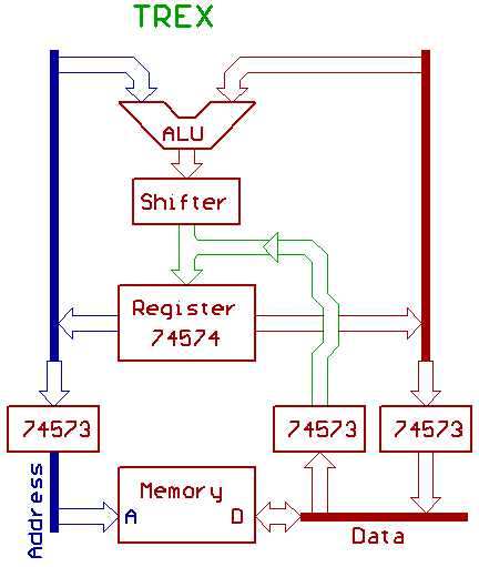
The basic design of our CPU shows some additional features:
74573 type transparent latches instead of the 74245 address and data bus buffers,
and a shifter.
The 747181 ALU is unable to shift right (PISC1 and Mark2 don't have a
"shift right" instruction), we did decide to insert a shifter between ALU
output and register file input.
A 74573 based transparent latch is used to read from the data bus,
it is able to bypass the ALU and to write directly into the register file.
We did decide to insert 74573 latches into the address and data outputs
of the CPU, a feature that might be nice for memory access with post_increment.
Post_increment means, reading a word from a memory address indicated by
a register, then incrementing said register.
With 74573 latches as in our design, there are two different approaches for
implementing this addressing mode, and they all take two cycles:
Either the "traditional approach", in which CPU places the address on the bus,
reads the data from the bus and writes it into the register file, and then
increments the address register in the next cycle.
Or to increment the register first, while freezing the address output latch in
the next cycle in which the data is fetched from the bus and written into the
register file.
[HOME] [UP]/ [BACK] [1] [2] [3] [4] [5] [6] [7] [8] [NEXT]
(c) Dieter Mueller 2007, 2008