Now to describe, how to build such an ALU with
logic gates.
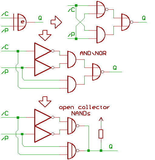
Open_collector_NANDs are a good choice, when using
PNP/NPN_transistors.
(Open collector means, that the output of the logic gate
is the collector of a NPN transistor that switches to GND.)
First, we focus at the XOR at the ALU output:
For the AND/XOR_example, an active AND gate (all inputs 1)
will turn the ALU output to 0.
When connecting the outputs of open_collector_NANDs together
to one pullup_resistor, they also work as some sort of
AND/XOR_combination.
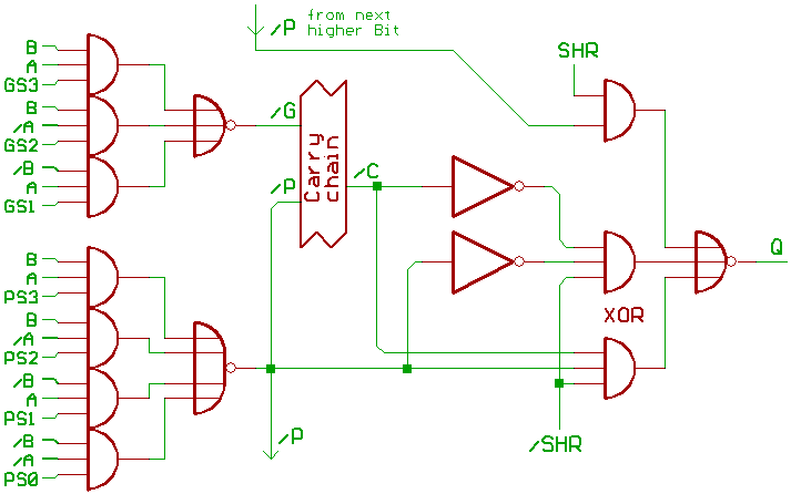
Would be nice, if we could integrate the shift_right_multiplexer
into the ALU_output.
Now an example, how to build this ALU with AND/XOR
(Without the unused GS0 gate):
Another example with open_collector_NANDs:
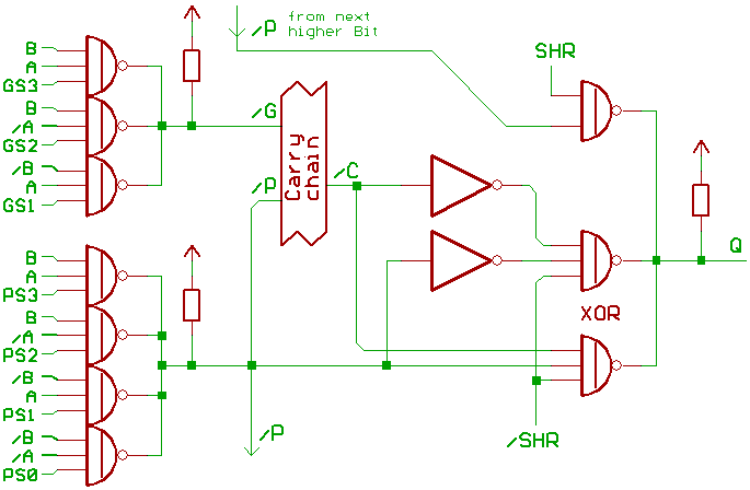
Note the SHR and !SHR control signal at the ALU output.
Looks like we could give the ALU an output_enable,
if we want to.
Yes, 10 open_collector_NANDs and 4 inverters
(two of them in front of the ALU to produce !A, !B).
That's all.
Can't optimize this design any further at gate level.
[HOME] [UP]/ [BACK] [1] [2] [3] [4] [5] [6] [7] [8] [NEXT]
(c) Dieter Mueller 2005