Thanks to Beregnyei Balazs for his reverse_engineering attempts.
(Open_collector/open_drain output inverters can be used
to build NOR_gates.)
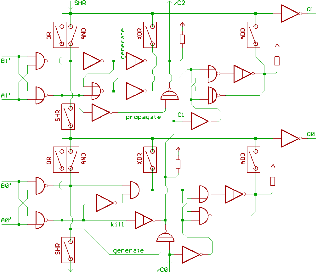
The input_multiplexers look as described two pages ago,
so I didn't draw them again.
What we called A is the special bus (SB), a bidirectional bus
that is used to read/write registers.
B would be the internal data bus (DB), it's mostly used
to read the external data bus through the data input latch.
The ALU output can connect through switches to the special bus,
and to the internal address bus A7..0.
(There are additional switches between special bus and internal
address bus A15..A8.
The ALU output also feds the BCD_correction_circuitry,
to write into the accumulator.
Note, that in the 6502 the pullup_resistors we had
at the ALU_inputs seem to be MOS transistors working
as current source during PHI2=1.
That's all for now.
On to part 3.
[HOME] [UP]/ [BACK] [1] [2] [3] [4] [5] [6] [7] [8]
(c) Dieter Mueller 2005