65816 board hardware
(C) 2010-2010 André Fachat
This page describes the hardware of the 65816 board.
In this section I describe the hardware design.
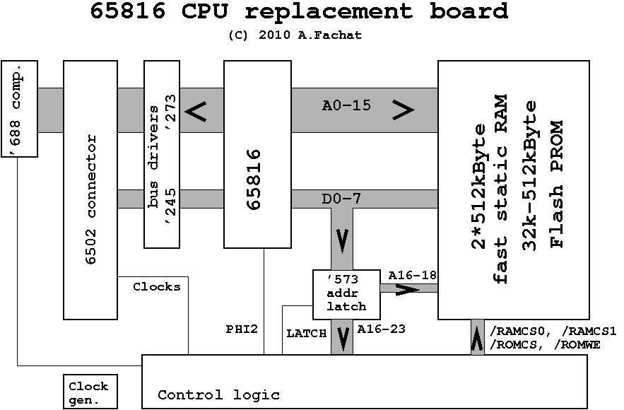
The board design overview (click to enlarge)
The board is actually quite simple. It has a CPU domain, with the CPU, RAM and ROM (incl. the '573 bank byte latch). It has a system domain, with the connection that goes into the 6502 socket on the system, and the '688 address decoder. And it has the address and data bus drivers that connect them, plus the CPLD glue logic.
CPU domain
The CPU domain actually is an own computer in itself, only that it lacks I/O capabilities. It has a ROM to store the program, plus RAM to actually work in it.
The '573 is the usual bank byte latch used for the 65816. You could actually
be moving this into the CPLD without board change, if the CPLD has enough space. The CPLD
already has the 8 data lines, and you have to redefine the three address lines
A16-A18 as output instead of input to the CPLD.
System domain
The system domain only has the 6502 connector and the '688 address decoder. The address decoder is actually used to decode the address of the CPLD's clock and control register, and to reduce the number of input pins needed on the CPLD.
Buffers
The buffers are used to decouple the slow system bus from the fast CPU bus. When the CPU does not need the system bus, it sets the buffers to read from system bus address zero. In fact the CPLD makes the address and R/-W only change exactly once a slow cycle. Either the address is set to the CPU address when a (slow) system access is performed, or zero, when the slow bus is not needed (as the CPU is running on fast clock).
Looking at the board layout you can see that of course it has the 65816 CPU, but also 2 RAM ICs with 512k each, and a socket for a ROM chip of between 32k and 512k. A 50MHz oscillator gives the clocks. Also the board has three driver ICs (2 '273, 1 '245), one latch (a '573), and a comparator (a '688). The main glue of the board is of course the Xilinx CPLD. The functionality of this IC is not fixed, but can be programmed using VHDL for example, a hardware description logic. It can contain the equivalent of a whole eurocard of standard logic ICs (depending on the ICs...)
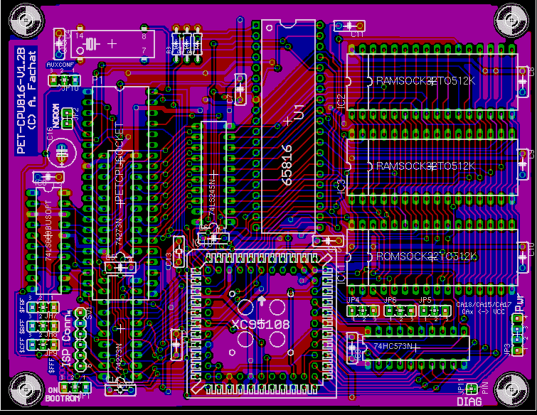
In the block diagram you can see how these ICs fit together.
The two RAM chips of course implement the 1MByte RAM. The ROM is in-place-programmable (when using the correct Flash-PROM that is - I am currently using an Atmel 29C010 128k PROM).
The '573 is the "usual" latch to capture the upper 8 address bits A16-A23 from the 65816's data bus during phi1. It is controlled by the CPLD to be transparent during phi1, then latch the value and hold it constant during phi2.
The '273s implement the address driver between the 65816 bus and the slow system bus (the 6502 connector). This has to be a '273 as this is the only IC that has a reset line to set all outputs to low. I use this to read from address 0 as long as the CPU works in the on-board RAM or ROM.
The '245 is the data bus driver. It decouples the 65816 and the system data bus.
The '688 finally is an address selector for address lines A4-A11 on the system bus. It is used to select two addresses in the I/O range for the CPLD's control and clock registers.
The board has a number of jumpers and connectors:
- JP1: BOOTROM - when set to on, the on-board ROM is mapped into the lowest 64k address space upon reset, so the board can take the system over
- JP2: NOROM - this jumper connects PIN 5 of the system (6502) bus connector to the CPLD. The Commodore PET uses this pin to disable the built-in ROMs. Currently not used in the CPLD.
- JP4: CA18 - allows to use a smaller ROM by connecting VCC to ROM pin 1
- JP5: CA17 - allows to use a smaller ROM by connecting VCC to ROM pin 30
- JP6: CA15 - allows to use a smaller ROM by connecting VCC to ROM pin 3
- JP7: IO1 - switches between $ExFF and $ExBF I/O for the CPLD
- JP8: IO2 - switches between $E(F/C)xF and $E(B/8)xF I/O for the CPLD
- JP9: IO3 - switches between $E(F/B)xF and $E(C/8)xF I/O for the CPLD
- JP10: AUXCONF - config input into CPLD, currently unused
- JP11: DIAG - single pin, output from CPLD - used for diagnostics signals
- P1: 6502 system bus
- JP3: pwr - additional power supply
- SV1: JTAG - programming connector for the CPLD
Return to Homepage
Last modified: 2014-08-11