How does the 65816 board work?
(C) 2010-2010 André Fachat
This page describes the inner workings of the 65816 board, what external and internal signals are there and how they work together. Also it explains the different parts of the VHDL code.
Table of content
Here the general design is discussed
The challenge...
As there are already 65816-based boards (like my CS/A65 65816 board) why should it be difficult to build a board to replace a 6502? Well, it's the timing! In my other 65816 board the actual system clock is derived from the 65816 fast clock in a synchronous way. But in a 6502 replacement no such synchronous clock is available. There are two clock domains, the system domain that feeds the board with a slow (1 MHz or 2 MHz for example) PHI0 clock - and the fast 65816 clock domain. These two need to be synchronized.
Unfortunately if two different clock domains interact, metastability can occur (see wikipedia link below for example). I.e. a signal might not settle on a defined high or low state for a considerable time when it is sampled directly during a transition for example.
There are two ways around this issue:
- synchronize the two clock domains such that clearly defined timing characteristics between the clock domains apply, and no clock shift occurs. You could do this with a PLL (phase-locked loop) for example.
- use an arbiter between the two clock domains as a means of communication between the two domains. Arbiters are still subject to metastability but with a multi-stage approach the mean time between failures can be set in the range of years or more.
Clock Synchronization
The clock synchronization has to happen on two places - from slow to fast and from fast to slow.
Let's first look at the fast to slow transition. When the CPU outputs the correct addresses
during an (initially) fast cycle, the CPLD logic detects a slow access and asserts the
isslow signal. This is sampled on the rising edge of the CPU clock
(which is in the fast domain at this time) to give the slowdetected signal.
The rising edge of the CPU clock is used as this is the time when CPU signals are guaranteed
to be stable. There has to be some safety margin to account for propagation delays in the
CPLD isslow generation though. Therefore the PHI1 phase cannot be too fast.
I found that it should be at least 50 ns.
Once slowdetected is asserted, the CPU clock is held high to await the actual
slow cycle. I.e. I don't use the CPU's RDY pin, but the 65816 feature that it can be stopped
indefinitely with PHI2 high.
As the fast and slow clocks are not synchronized, the detection that a slow access should be done can be anywhere during the slow clock cycle. It could be during PHI1, PHI2 close to any of the transitions, anywhere. That's where the "arbiter" kicks in.
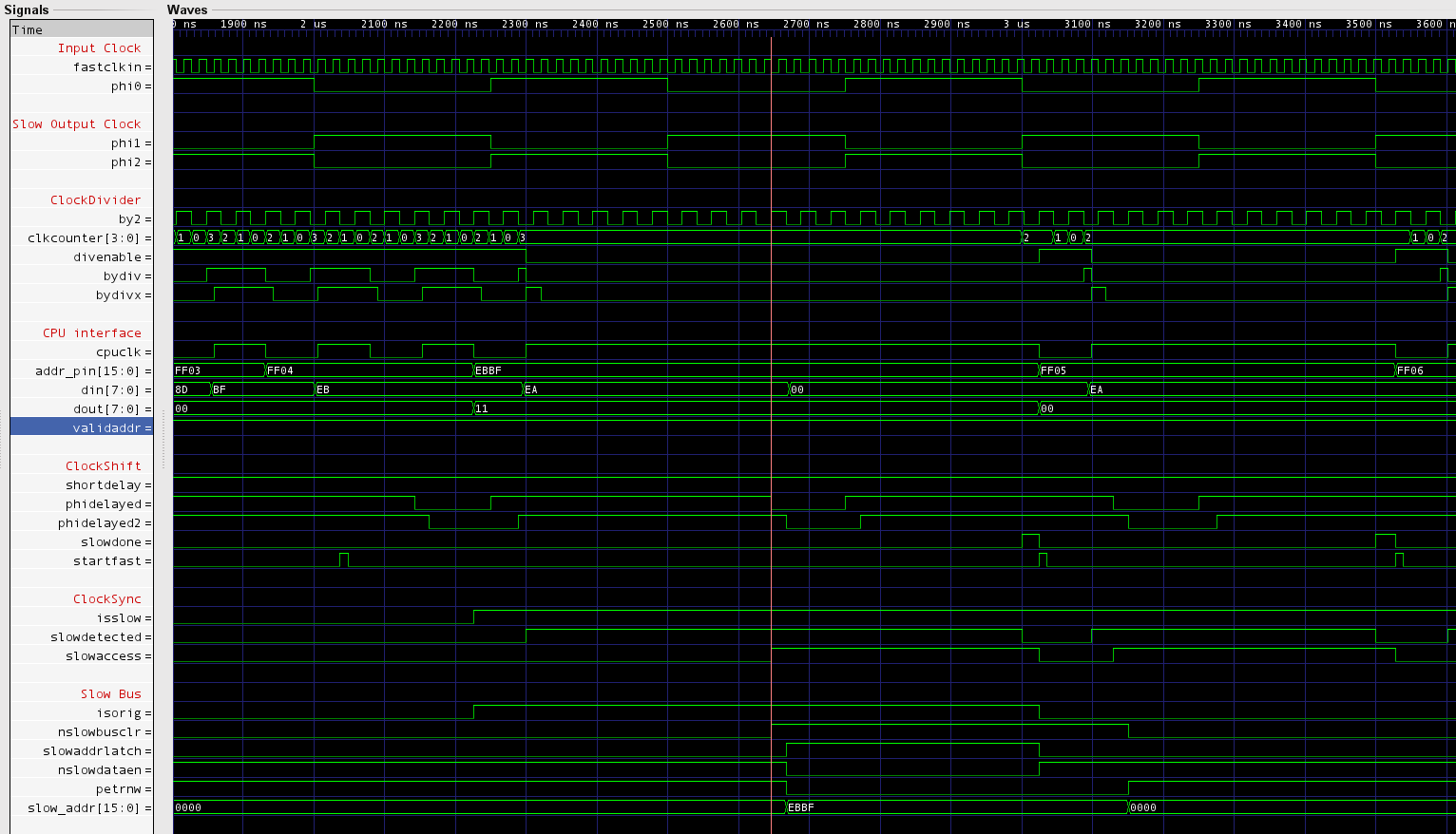
General timing structure
In this diagram you can see that the first slow access is detected at 2300 ns, in the middle of a slow cycle (PHI0/PHI2 high). The actual slow access thus has to wait for the next slow PHI1 cycle to actually start.
In the timing diagram you also see a signal called phidelayed. This plays a key role
in the synchronization mechanism. This signal is the slow PHI0 input, but delayed for a certain
amount of time (and OR'd with PHI0, see 2 MHz operation below).
The falling edge is important here. phidelayed is delayed such that the falling
edge is far enough before the rising edge of PHI2 to allow for address bus setup times.
Therefore when phidelayed
goes low, and a slow cycle is already detected, an actual slow cycle starts.
More concrete, when slowdetected is detected on a falling edge of
phidelayed, then slowaccess is asserted to actually start a slow
cycle. To avoid any race condition (such as one signal derived from slowdetected
having a different propagation delay than another and then only one of these being latched
at phidelayed going low), this signal is then used as "single point of thruth"
signal to enable the slow bus (only if the slow access actually goes to the slow bus, and not to
the board's RAM or ROM). These signals are then latched with phidelayed2 going low
which comes 20 ns after phidelayed. The nslowbusclr,
slowaddrlatch, nslowdataen and rnw then determine the
state of the slow bus (details see below).
After the slow access, when PHI2 goes low, a small pulse signal startfast
is generated to then restart the fast access. This pulse actually enables the fast clock
counter again (divenable) so that the fast clock starts with a fresh,
PHI1 cycle (i.e. PHI2 low). In the diagram you can actually see that the next cycle
is also detected as a slow cycle, but it is not detected as going to the original system bus.
Jitter
As the two clock domains are not completely in sync, there is some jitter that appears
between the slow domain signal (PHI2) and its fast clock domain counterpart
(phidelayed). I.e. the timing interval between PHI2 going low and
phidelayed going low is not constant, but changes in the range of a fast clock
cylce, i.e. 20 ns. All other timing values must take this into account.
Also there is some jitter when the slow cycle ends. A PHI2 going low the slowdone
signal is asserted. This signal is used to reset the slowdetected signal, so this
goes low directly with PHI2 going low. This pulse must be long enough, so startfast
that ends the slowdone pulse must be at least 10 ns, better as I use it
20 ns after PHI2 goes low. startfast has some jitter, though. It is derived
from the phidelayed shift register line, so it is subject to the same jitter
as phidelayed.
Original bus access
The CPLD control interface for the original bus consists of these signals:
nslowbuslcr- if low, set the address lines to zero (as long as CPU does not need the original busslowaddrlatch- on a rising edge of this signal the CPU address bus values are latched and put on the original system bus. Must be at least about 20 ns behindnslowbusclrgoing high, to allow the '273 ICs to recover and latch the correct address.nslowdataen- if low, connect the CPU data bus with the system data busrnw- this is the system bus read/not write line. You cannot connect this directly to the CPU, so in the CPLD a circuit similar to the '273 is emulated for the read/not write line
The startfast signal is actually derived from two other signals,
startfastr and startfastw, one for read and the other one
for write accesses. As this signal determines when the CPU continues with a new cycle,
you could actually delay this differently for read and write cycles. Originally I thought
that I need to delay further for write cycles to make the data bus hold time longer.
As the 65816 is very fast, that could be a problem so I anticipated that. During the tests,
however, it showed that I had to delay the read access as well. That could have been
due to the way I then created the signals to clear and latch the slow address bus.
As I have changed that I currently do not see any need to delay read cycles anymore.
So there is still room for experimentation.
Bogus cycle elimination
On quite some opcodes the 6502 CPU does memory accesses that are actually
not used, so called bogus cycles. It does them when it needs time to internally compute
an address value for example (e.g. when crossing page boundaries etc). The original
6502 has no way of telling the external system whether a cycle is valid or not.
But the 65816 has such a way, using the VPA and VDA signals.
Therefore is is possible to hide a bogus cycle from the original system.
Assume that the system is running in slow memory only. Normally the CPLD would
detect the slow access on the next fast cylce (after the first PHI1 phase after
the previous slow access), and wait for phidelayed going low to initiate
a real slow cycle.
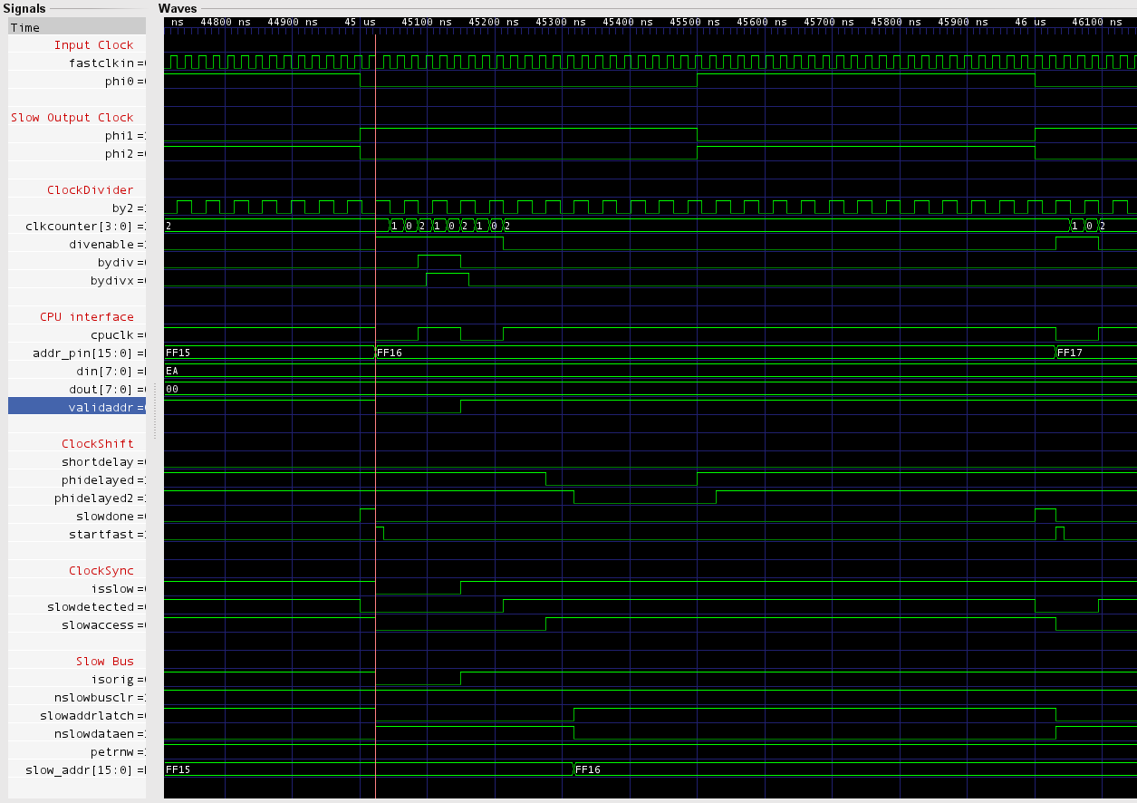
Hiding bogus cycles
but when the cpu access is not valid, there is no need to wait for the actual slow cycle.
instead the cpu can continue with the fast cycle and then begin a new cycle.
this new cycle is then (most of the times) a valid one. So when the complete invalid cycle
plus the phi1 phase of the following valid cycle fit between phi2 going low and
phidelayed going low, the slow system only sees two consecutive - valid -
cycles, and the invalid cycle is hidden!
You can actually see an invalid cycle being hidden in the diagram linked here. The CPLD
builds the validaddr signal from VDA and VPA. When
this signal goes low, the cycle is not valid, which happens shortly after time 45us in
the diagram, where the red marker line is.
2 mhz operation
To hide bogus cycles, the time interval between PHI2 going low and phidelayed
going low must be long enough. Unfortunately, when the system is running at 2 MHz, this
time interval is too long: there is not enough time between phidelayed going
low (starting a slow access) to allow for the address setup times on the slow bus.
In fact the falling edge of the phidelayed actually runs into the
following PHI2 phase! That is actually why phidelayed is OR'd with PHI2, so
that in this case the system does not hang.
That is where the FASTMODE clock register bits comes in. It is set by default
and reduces the phidelayed delay such that the system actually works with
2 MHz. But there is a cost - you cannot hide bogus cycles anymore.
clock duty cycle
Maybe you have already wondered how I actually get to a CPU clock frequency of 10 MHz. There actually is a trick involved.
Why is this so difficult to achieve with a 50 MHz clock signal? Because the clock is divided by an odd value, 5. Going from frequencies to clock cycle lengths, going from 50 MHz to 10 MHz means to go from a 20 ns clock cycle to 100 ns, i.e. 5 times as much. But normally clock dividers work on a fixed transition on the input signal. I.e. when using 5 cycles of the input clock I would only be able to have something like 2 cycles low and 3 cycles high. I had actually tried this by changing the clock latch value loaded into the clock counter by one depending on the clock state. The CPU would work with faster speeds (it's rated 14 MHz) so 40 ns low is ok, and the RAM would work with 60 ns ok.
However, as I have already written above, this did not leave enough time for the CPU to put up the addresses and the CPLD to actually use the address for address decoding. What could I do? Here comes the trick. I delayed this asymmetric clock signal by 10 ns by using the opposite edge of the fast input clock, then AND'ed the two signals. Alas, a clock signal with 50 ns low and 50 ns high phase.
Admittedly this signal is out of specs for the static RAM chip I use, which is rated 55 ns access time. Using the burn-in test however, I found it still works. I might get me a faster RAM IC though.
in this section i will describe the main structure of the vhdl code that implements the logic in the cpld. i will also go into ways of efficient testing as i experienced while developing the board.

vhdl structure
vhdl defines that logic is separated into modules. each module has input and output signals that define the "interface" of the module. in general you can think of these modules as being similar to logic ics. these ics resp. modules are then plugged together in higher level modules, using the input and output signals.
so i have separated the cpld logic into different modules as well, which i am going to explain here. the different modules and their structure is shown in the side image.
pet816.vhd
this module is the top level module. its input and output lines are the ones that are used on the cpld pins. it does not actually contain any logic. instead it only passes the signals to the core module. in addition to that it also defines the power-up values of the clock and control registers, that are passed to the core module.
the power-up values for the registers are defined in this module, so that in a debug setting i can define different power-up values for the registers without changing the core module.
core.vhd
the core module is the one that holds all the other parts together. its input and output signals are the ones for the cpld pins, but additionally contains the power-up values for the clock and control registers.
internally it wires all the other modules together. mostly it does this by wiring signals from one module to the other. only a few signals are created in the module itself.
the two most important signals generated here are isslow, and isorig.
the isorig signals goes true when the address selection signals from the
systemmap module (plus some control register values) indicate that the cpu access goes
to the slow system bus, using the 6502 bus interface to the base system.
isslow goes active when a slow system access is detected using the cpu
signals - addresses, vpa/vda (in form of the validaddr signal), r/-w - control
register bits and more. it is an asynchronous signal that appears when the cpu signals
fulfill the appropriate conditions. it is then clocked in the clocksync module.
systemmap.vhd
the systemmap generates signals for the different memory areas. it determines where in the memory map the i/o and the video memory areas are. it also determines where the mirror ram (for the lowest 64k) and the system mirror are. this is the only module that needs to be replaced for a different type of system (at least in theory).
clockdivider.vhd
this module creates the main clock signals. it gets the 50mhz input clock and divides
the clock signal by 2 (divby2),
as well as by the value given from the clock register.
the latter signal (masterclk) is then used to generate the
actual cpu clock. the clock divider has an enable input that resets the clock signal.
this is used to restart the fast masterclk with a full phase 1 (phi1 high,
phi2 low) after a slow access.
ClockShift.vhd
The ClockShift module uses the masterclk and divby2 signals
to to delay the slow system clock by defined delay times. The resulting signals
phidelayed, phidelayed2 and fastr/fastw are used
to synchronize the CPU with the slow system clock.
ClockSync.vhd
This module controls when the CPU is doing a slow memory access (be it orignal system bus, or
on the board's fast bus - ROM or the SLOWCLK control register bit is set).
The slowdetected signal is the isslow signal clocked by the
rising edge of the CPU clock and signals that the CPU waits for a slow memory access.
When the correct timing allows to start a slow access, the signal slowaccess
then enables the slow access cycle. The slow cycle is ended with the startfast
input - which is generated in the Core module from the fastr/fastw shift
module outputs. But startfast is only effective when the system's RDY signal
allows to end the cycle.
ControlRegister.vhd
The control register module not only contains the control register, but also the clock register. Its input signals contain the power-up init register values, as passed from the PET816 module. Its output are the various control register values. Unfortunately the registers are only write-only at the moment
BoardMemSel.vhd
This module creates the select lines for the onboard RAM and ROM ICs, including the ROM's write-enable (for the programming).
Writing VHDL is one thing, making is work is another thing.

VHDL test setup
Test Setup
To be able to test effectively and efficiently you need to take some care and create a good setup. The picture on the right shows my test setup. As you can see the Core and its contained modules are exactly the same as in the CPLD setup above. The PET816 module is left out though, but that gives the opportunity to pass different, test-related power-up values to the registers.
The main test setup module is the PET816 Test Bench (TB) module. It simulates the actual system, i.e. it wires together the actual CPLD Core module with a 6502 CPU, some RAM and the external test parameter module. In the test bench the hardware of the 65816 board is simulated in a basic way. For example the '273 address latches are emulated to simulate the correct system bus address values (and therefore to read the correct data values e.g. from ROM). The test bench also contains the clock generators for the internal (50MHz) or system bus clock (1MHz or 2MHz depending on config option).
The outermost module is the actual test. It contains the test parameters and the test ROMs and feeds these values into the actual test bench. Test parameters are the initial register values for example. The ROM has a RESET vector, and contains NOP operations as default value. Only the code that is needed for the test is put into the emulated ROM. This way the only module that is specific to a certain test case is the outermost module and is actually implemented as a separate file for each test case.
Test Execution
In my VHDL project setup, which is a Xilinx ISE Webpack project, I have a subdirectory called
testsuite. In this directory I have created (in further subdirectories) the
test bench and test case codes. The test bench as well as the free6502 CPU VHDL is in the
src subdirectory. The test cases are in the testbench directory.
The tests work in a Linux (should work on any Unix) environment and requires the
make, ghdl and gtkwave programs installed.
ghdl is a VHDL simulator based on the GNU Compiler Collection (GCC).
gtkwave is a viewer to view the output of the ghdl simulation.
The signal images shown above are made with this tool.
Running the tests is done by running
make ctrlor
make hbogin the testsuite directory, to run the
ctrl or hbog test cases
respectively.
Clock Testing
As described above the synchronization of the two clock domains can lead to problems, and one common error here is to do testing only with synchronized test clock generators - that are synchronized and do not show real-world clock drift.
Therefore I don't use an exact 50 MHz clock in the emulation, but drift about 1 ns per clock cycle. This allows me to scroll over some execution cycles and get a picture of whether there are problems in the clock synchronization.
Test Timing
On the ctrl test case I ran into a problem when I started to actually
gate the ROM output with the CPU clock. The CPU latches the data bus values
at the falling edge of the CPU clock. In the simulation however, the ROM output
was already set to open before the CPU gated the values, thus it did not work.
So here I started to work onto actually simulating delays with VHDL. In the testbench I created a new signal
cpuclk_del <= transport cpuclk after 5 ns;This code takes the
cpuclk signal and delays it for 5 ns. Using
this delayed clock signal to determine the CPU data input from the ROM output,
the VHDL simulation allows the CPU to latch the ROM data when its clock goes low
and before ROM output goes into tri state:
        if (cpuclk_del = '0') then
             	-- RAM/ROM data switch off time
                core_data_in <= transport "ZZZZZZZZ" after 5 ns;
        else
                if (cpuaddr(15 downto 12) > "1000") then
                        -- ROM access time (from_data is without delay)
                        core_data_in <= reject 10 ns inertial from_data after 70 ns;
                else
                        -- RAM access time (from_data is without delay)
                        core_data_in <= reject 10 ns inertial fram_data_out after 50 ns;
                end if;
        end if;
In this code there also is a the reject/inertial/after command.
This construct allows to reject spikes in the signal, here a 10 ns spike will
be ignored (the value after the reject). Then the signal is
delayed by the time values after the after statement.
Please keep in mind that an if has an immediate response, i.e. there is no
delay or inertial reject involved. If you want to delay the effect of an if
statement, you have to create a delayed signal that you have to use in the if
condition as I have done here with the cpuclk_del signal.
I have currently done only a very basic simulation. With more test cases (if necessary) I expect to get more accurate here and use more of the timing delays.
As far as I understand the transport and inertial delays are ignored when doing the actual synthesis, but I haven't tried it so far, though.
Return to Homepage
Last modified: 2014-08-11