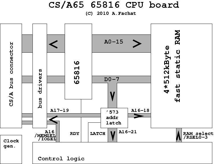
CS/A 65816 V2 CPU
This board implements a 65816 CPU board for the CS/A computer. The CPU runs on eight times the bus clock speed, i.e. for a 1 MHz bus, the CPU runs on 8 MHz. Currently only 1 MHz bus/8 MHz CPU is supported though. It features up to 1.5 MByte fast RAM that is used at CPU speed, and 512k ROM. To access the ROM, the bus memory or the I/O, the CPU is slowed down to bus clock speed with the RDY pin.
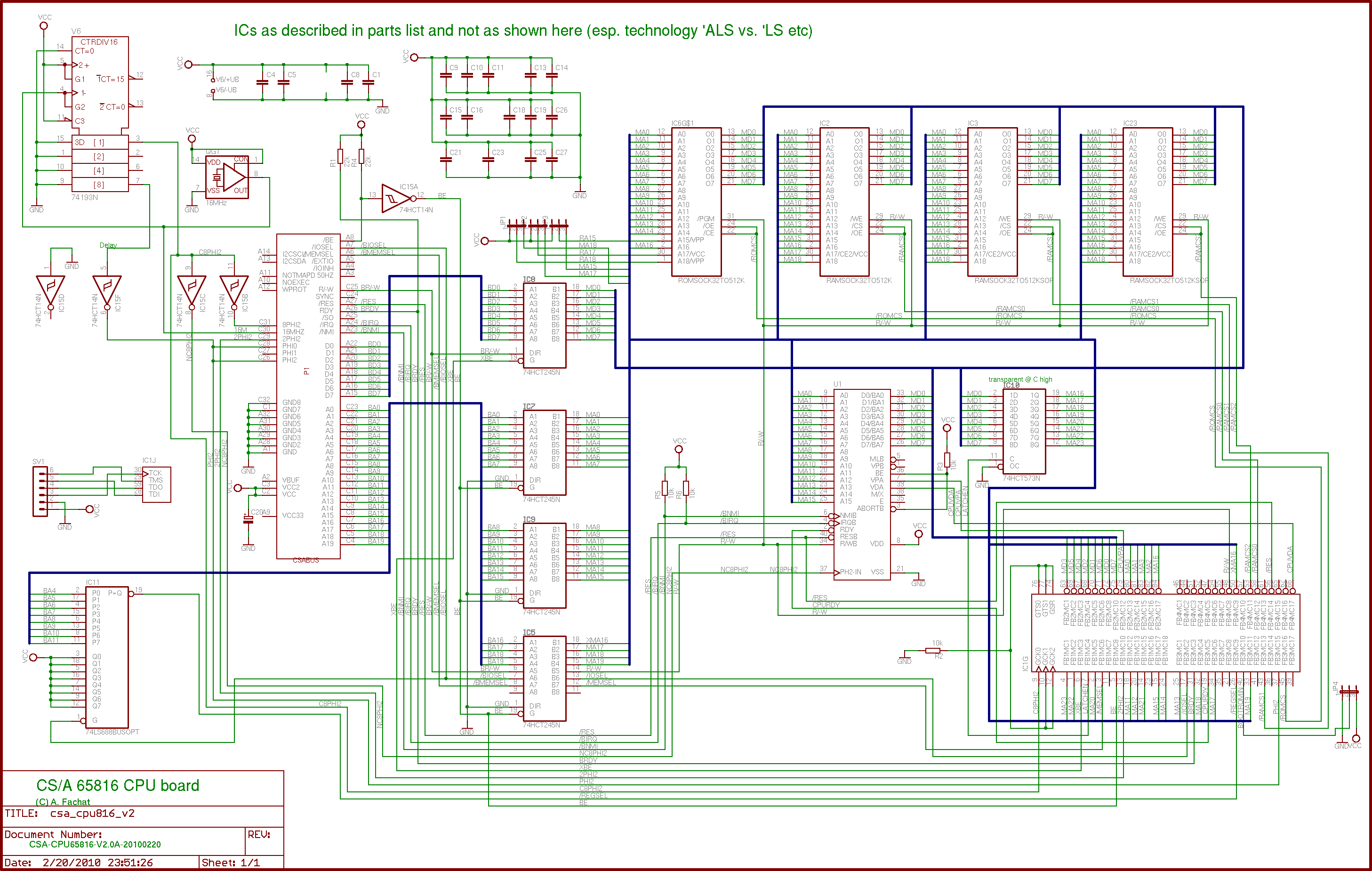
This board uses a Xilinx CPLD as the main logic element. Basically all of the logic shown in the version 1 board has been moved into this chip. If you don't have access to a programmer, or don't want to use a CPLD you can still look at the version 1 board - it only has a GAL for timing reasons.
CPLDs and other programmable logic is even today already mostly available in 3.3V or even lower supply voltages and SMD packaging. I used a Xilinx XC9572 CPLD, a 5V version which is still available (probably as "new old stock") in PLCC packages. Although - after looking again into the WDC datasheets - I could have probably done a 3.3V design with voltage converters to the bus (the 65816 runs with 3.3V, although a bit slower).
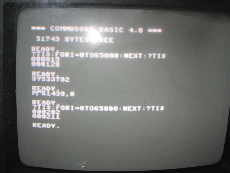
Screenshot of a timing measurement. On the top of the screen you see the result of the original speed, then copying (SYS33792 where I assembled the test to), then POKEing the control register to fast speed and measuring again.
With this board I was able to achieve a speed increase of over 8 times compared to the 1MHz system :-)
- 2010-12-22 The schematics and VHDL is updated and fixed. It is now compatible to the PET816 board (with the exception of the speed register), so the same programs run on both systems.
Table of content
When building the version 1 board I found that it is very tedious replacig parts, cutting traces and soldering new connections each time I had to test something. So I decided to try out more integrated programmable logic (more integrated than a GAL that is).
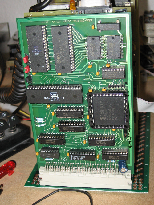
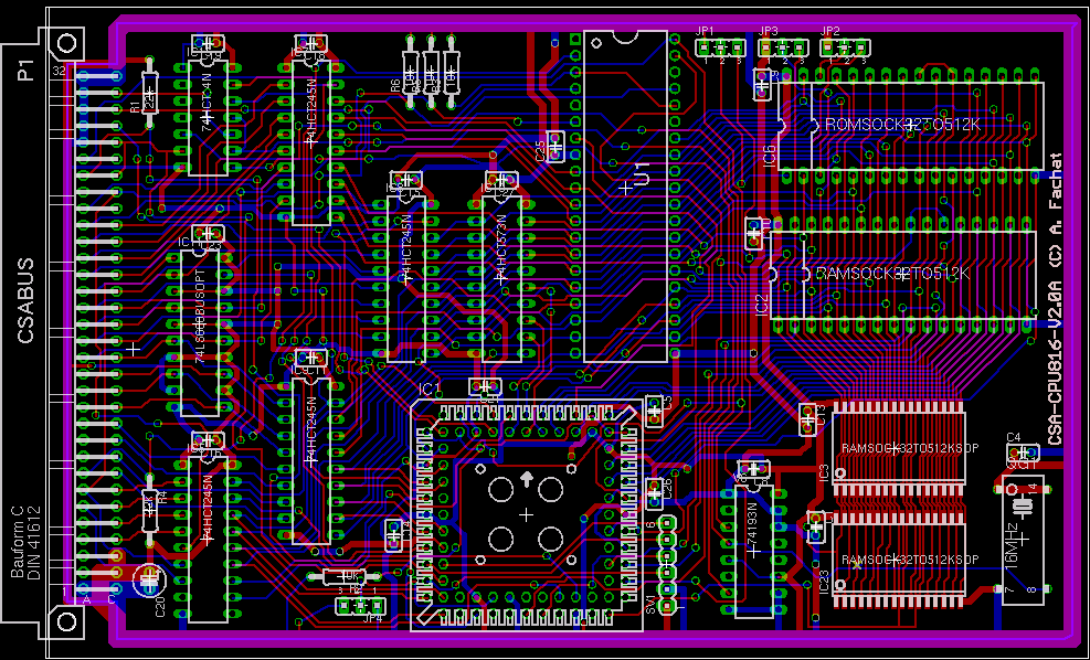
The 65816 CPU board version 2 with the PLCC CPLD logic chip.
This resulted in the CPLD programming environment giving some warnings about latches it detected, as well as combinatorial feedback loops. But yes, that's how the version 1 works, using well-placed and controlled flip-flops, and also feedback loops. So I ignored the warnings.
Using a CPLD allowed me to introduce a few more features:
- A control port to control the memory mapping (something which was very crudely done by accessing RAM3 on the version 1 board
- A more consistent memory mapping, mapping the RAM0 "under" the original 64k for write accesses
- Write protection for fast RAM in the upper ranges of the lowest 64k - so you could replace/test other ROMs
- 512k in-system-programmable Flash ROM, the lower 64k of which can be used to boot the system (jumperable)
After finding this issue, the rest of the timing issues were solved quickly by comparing what I had in the CPLD with what was working in the version 1 board.
There is one caveat though - the 2Phi2 generation is using more time in the CPLD so that it is delayed compared to the Phi2 signal. Using a 74LS14 instead of the 74ALS14 inverter as I had before delayed the bus Phi2 signal appropriately. The next step in the desig will be to integrate the clock counter and the inverter into the CPLD as well, then generating synchronized clocks, which should make the problems go away. But the first goal was the reproduction of the version 1 board with a CPLD and it worked :-)
By the way, the PET bell tone already becomes noticably faster even if you only speed up the bogus 6502 CPU cycles (which results in them not showing on the 1MHz bus).
The memory map is relatively simple, only the lowest 64k are more complicated:
| Memory area | Range | no BOOTROM, no SLOW64k | BOOTROM, no SLOW64k | no BOOTROM, SLOW64k | Comments |
|---|---|---|---|---|---|
| $000000-$007fff | 32k | FastRAM | BootROM | CS/A bus | Writes always also go to FastRAM (write through) |
| $008000-$0087ff | 2k | CS/A bus (video memory) $18000-$187ff | Note: If the FASTVREAD control register bit is set, only writes go to the system bus (and write through to FastRAM), but reads only go to FastRAM. | ||
| $008800-$00e7ff | 24k | FastRAM | BootROM | CS/A bus | Writes always also go to FastRAM (write through) |
| $00e800-$00efff | 2k | CS/A bus (io) | Writes always also go to FastRAM (write through) | ||
| $00f000-$00ffff | 4k | FastRAM | BootROM | CS/A bus | Writes always also go to FastRAM (write through) |
| $010000-$17ffff | 1472k (3*512k-64k) | FastRAM | |||
| $180000-$dfffff | --- | ||||
| $e00000-$efffff | 1024k | CS/A bus (memory) | |||
| $f00000-$f7ffff | 512k | FastRAM mirror of $000000-$07ffff | |||
| $f80000-$ffffff | 512k | ROM | |||
Video and I/O are always mapped to the CS/A bus. The video area is mapped in the second 64k on the CS/A bus, where normally the VDC card with its video memory is located. I/O is mapped on the /IOSEL select line on the CS/A bus.
This section describes the control port for the CPU board. The port is located at $EBFF in the I/O area and is (currently) write-only (It can be relocated to $EFFF via jumper, but due to incompatibilities with my CS/A setup I decided to use $EBFF as standard location). The different bits are used as described in this table:
| Bit | Value | Name | Description | Init value | Notes | |||||||||
|---|---|---|---|---|---|---|---|---|---|---|---|---|---|---|
| 7 | 128 | PRGROM | When set, allows write access to the built-in ROM. Note that specific algorithms are required to do the programming, random access does not work | 0 | ||||||||||
| 6 | 64 | BOOTROM | When set, the lowest 64k CPU address space are mapped to the built-in ROM (except video and I/O, see above) | Bootrom jumper | Note this allows to unmap the system ROM after boot by setting this bit to 0. Only the initial value is taken from the Bootrom jumper. | |||||||||
| 5 | 32 | SLOW64K | When set, the lowest 64k CPU address space are mapped to the CS/A bus (except video and I/O, see above) | 1 | ||||||||||
| 4 | 16 | SLOWCLK | When set, use slow access even on fast memory | 1 | ||||||||||
| 3 | 8 | HIDEBOGUS | When set, hide the CPU's bogus cycles - as indicated by VPA and VDA both 0 - from the system bus when possible. | 1 | ||||||||||
| 2 | 4 | FASTVREAD | When set, read the video RAM area from the fast RAM (writes still go to the slow system RAM) | 1 | ||||||||||
| 1,0 | 2,1 | WPROTECT | Write protect upper parts of the lowest 64k of FastRAM
| 00 |
This section describes some notes and possible future enhancements of the board. Of the possible enhancements from version 1, actually only the too small GAL has been addressed. The following are thus mostly still from the version 1 list:
1) DRDY is only used to disable /SLOWMEM, so that RRDY
is only a pulse that can be sampled at the rising edge of 8Phi2 (it has been used
for other purposes in the first - faulty - design). Maybe it can be replaced with RDY.
2) The GAL has been replaced by a CPLD - ok!
3) Similar to the PET 8296 the whole timing generation could be modernized
.
The 8296 uses a '163 synchronous timer, the input of which is given to a small PROM,
and the output of that PROM again is clocked by the 16MHz clock. This results in absolutely
synchronous clock signals, which makes timing much easier. In the current design
we would need a register clocked at 8Phi2 and another one at /8Phi2.
This could probably be done easily in the CPLD.
4) Currently BRDY, the CS/A bus RDY line is sampled at the end of
Q7, when XQ7 is sampled by 8Phi2, 65ns before
Phi2 goes low. This may or may not be a problem for slow memory that uses
RDY.
5) The control port was planned to be read-write, but I only managed to make it write only. This could be fixed.
Simple test suite
xa cross assembler with the -w
switch to allow 65816 code.
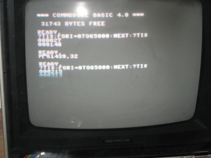
Remove bogus accesses: Screenshot of a timing measurement. On the top of the screen you see the result of the original speed, then POKEing to ignore bogus CPU accesses and measuring again. See about 14% speed increase.
| test1.a65(copies all of the lowest 64k but the I/O area onto itself, so it is automatically written to fast RAM ) |
Version: 2.0E
Status: prototype
Notes
This version adds a jumper to define the control port address.
Also the new /ROMOE signal enables writing the ROM in-system...
| |
| The layout has not been tested, I fixed my 2.0A version up to 2.0E. |
Files
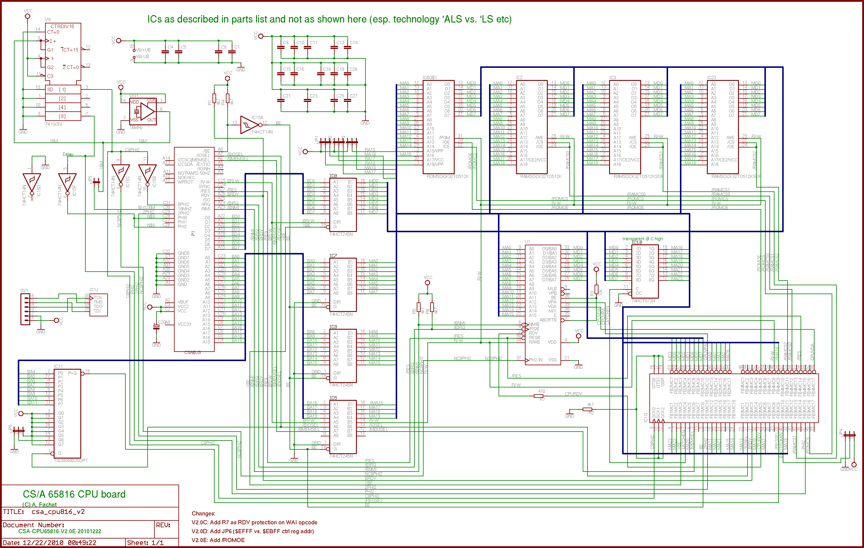
| csa_cpu816-v2.0e.sch | |
| csa_cpu816-v2.0e-sch.png | |
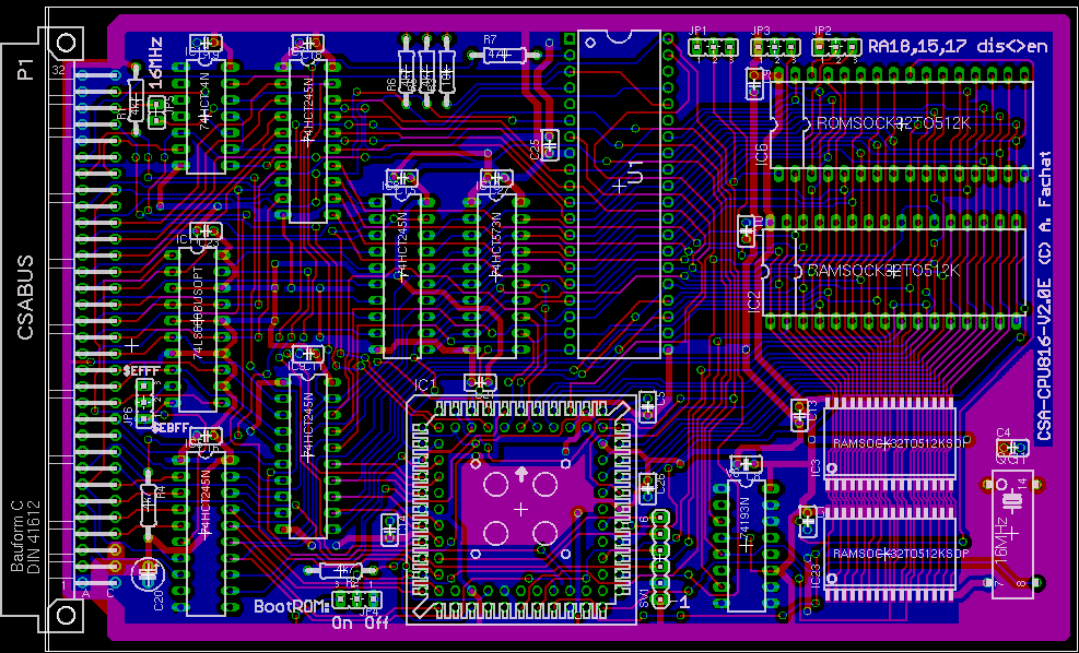
| csa_cpu816-v2.0e.brd | |
| csa_cpu816-v2.0e-brd.png | |
| csa_cpu816-v2.0e.parts | |
| csacpu816-v2.0e.vhd(CPLD VHDL source) | |
| csacpu816-v2.0e.ucf(CPLD constraints file (pin mapping)) | |
| csacpu816-v2.0e.jed(CPLD compiled source) |
Version: 2.0C
Status: deprecated
Notes
| Compared to the 2.0B board it adds a protection resistor for the RDY signal. When the CPU executes a WAI instruction, RDY is pulled low, this may overload the chip drivers, thus the resistor. Untested though. | |
| The in-system ROM programming is not working. | |
| The layout has not been tested, I fixed my 2.0A version up to 2.0B. |
Files
| csa_cpu816-v2.0c.sch | |
| csa_cpu816-v2.0c-sch.png | |
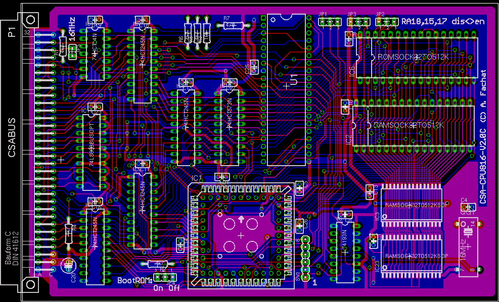
| csa_cpu816-v2.0c.brd | |
| csa_cpu816-v2.0c-brd.png | |
| csa_cpu816-v2.0b.parts | |
| csa_cpu816-v2.0b.vhd(CPLD VHDL source) | |
| csa_cpu816-v2.0b.ucf(CPLD constraints file (pin mapping)) | |
| csa_cpu816-v2.0b.jed(CPLD compiled source) |
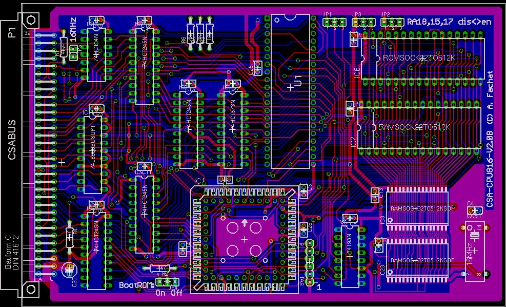
Version: 2.0B
Status: deprecated
Notes
| Compared to the 2.0A board it fixes the timing bugs. | |
| The layout has not been tested, I fixed my 2.0A version up to 2.0B. |
Files
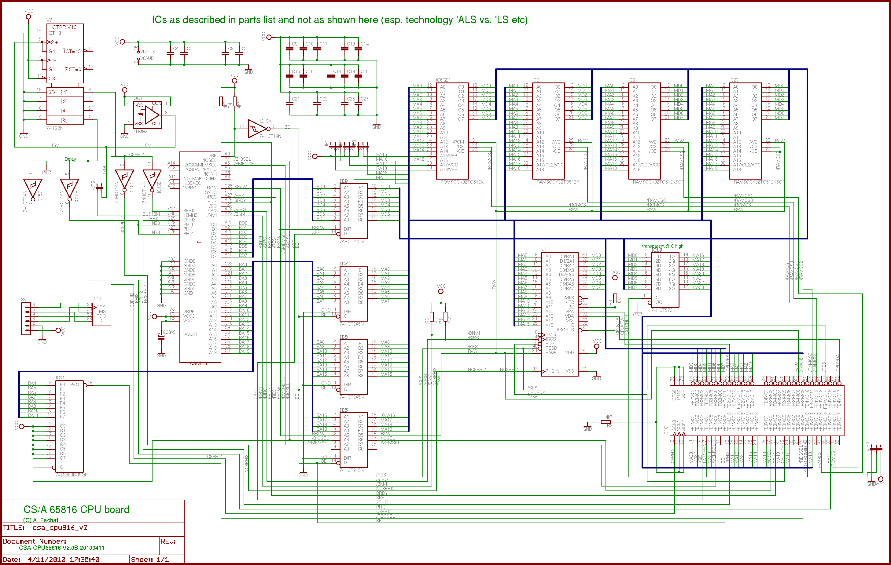
| csa_cpu816-v2.0b.sch | |
| csa_cpu816-v2.0b-sch.png | |
| csa_cpu816-v2.0b.brd | |
| csa_cpu816-v2.0b-brd.png | |
| csa_cpu816-v2.0b.parts | |
| csa_cpu816-v2.0b.vhd(CPLD VHDL source) | |
| csa_cpu816-v2.0b.ucf(CPLD constraints file (pin mapping)) | |
| csa_cpu816-v2.0b.jed(CPLD compiled source) |
Version: 2.0A
Status: deprecated
Notes
| There are a few timing issues, and the main bug is that the counter counts the wrong way - so the phase between phi2 and 8phi2 is wrong. |
Files
| (Picture of the assembled board) | |
| csa_cpu816-v2.0a.sch | |
| csa_cpu816-v2.0a-sch.png | |
| csa_cpu816-v2.0a.brd | |
| csa_cpu816-v2.0a-brd.png |