Blitter - how it works
(C) 2007-2011 André Fachat
This page explains how the CS/A Blitter works.
- 2010-09-17 Started this page
Table of content
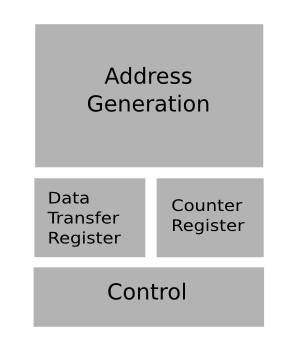
The blitter architecture is based on a CPU-like architecture. It uses registers connected to shared busses, and a single ALU between the busses.
The main components are:
- Address generation: creates the blitter addresses to read and write the data bytes.
- Data transfer register: The register to store the data read in the first transfer cycle, and to provide it in the second cycle
- Counter register: counts down the number of bytes to transfer. Also compares the number of bytes to zero, to get an end signal.
- Control: state control, and a logic array to control all the registers and buffers
Address Generation
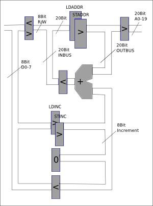
The address generation components are:
- LDADDR/STADDR: address registers for load and store addresses
- LDINC/STINC: registers for address increment
- ALU: Adder to add the address and the increment
- ZERO: zero increment (see below for the purpose)
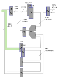
- Address data buffer: connects the INBUS to the CPU data bus. Note that this is actually three 8-bit buffers, where one byte at a time can be accessed (denoted by the "8Bit" in the diagram)
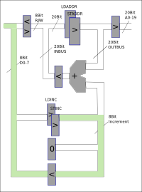
- Increment data buffer: connects the Increment bus to the CPU data bus
- Address buffer: drives the address from OUTBUS to the system address bus
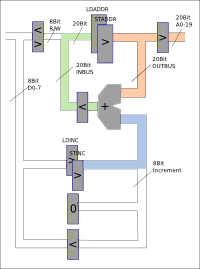
These components are connected together by three busses:
- INBUS: The INBUS is called that as it feeds a new address value into the load and store address registers. The value can come from the ALU output or from the CPU data bus.
- OUTBUS: The outbus holds the output from the load and store address registers. Its value is put on the actual address bus during a fetch or store operation. The value from this bus is at the same time also fed into one side of the ALU adder.
- Increment: This bus holds the output of the increment registers, resp. the zero increment value. Its value is fed into the second ALU adder input, but can also be read from the CPU data bus.
Together these components allow to do the actual data transfer, as well as the address increment of the address registers in a single cycle. The same, shared, ALU and bus components are used in both cases, when the data is fetched and when it is stored. This helps to keep the required board space small enough.
The actual circuit also features a control register, that allows to set the adder's carry, and the additional bits necessary to extend the increment value to a full address width. This for example allows:
- incrementing 256 byte (page): set the carry and use an increment value of $ff
- decrementing: set the carry, use inverse (EOR #$FF) of the value to subtract as increment and set the complement bit (upper increment bits). For example to substract by one, set the carry, use $FE as increment value and setting the complement makes the increment to $FFFFE. You can also clear the carry and use $FFFFF as increment of course.
This section explains the operating modes of the address generation.
Return to Homepage
Last modified: 2011-04-29